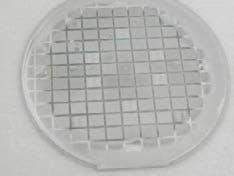
Gallium-nitride (GaN) and Indium Gallium-nitride (InGaN) Technology Targets Fast-growing Markets for Wearable Vision Systems GRENOBLE, France – CEA-Leti announced that it has demonstrated a path to fabricating high-density micro-LED arrays for the next generation of wearable and nomadic systems in a process that is scalable to the IC manufacturing process. The high-brightness, enhanced-vision systems such as head-up and head-mounted displays can improve safety and performance in fields such as aeronautics and automotive, where the displays allow pilots and drivers to receive key navigation data and information in their line of sight. For consumers, smart glasses or nomadic projection devices with augmented reality provide directions, safety updates, advertisements and other information across the viewing field. LED microdisplays are ideally suited for such wearable systems because of their low footprint, low power consumption, high-contrast ratio and ultra-high brightness. Leti researchers have developed gallium-nitride (GaN) and indium gallium-nitride (InGaN) LED technology for producing high-brightness, emissive microdisplays for these uses, which are expected to grow dramatically in the next three to five years. For example, the global research firm MarketsandMarkets forecasts the market for head-up displays alone to grow from $1.37 billion in 2012 to $8.36 billion in 2020. “Currently available microdisplays for both head-mounted and compact head-up applications suffer from fundamental technology limitations that prevent the design of very low-weight, compact and low-energy-use products,” said Ludovic Poupinet, head of Leti’s Optics and Photonics Department. “Leti’s technology breakthrough is the first demonstration of a high-brightness, high-density micro-LED array that overcomes these limitations and is scalable to a standard microelectronic large-scale process. This technology provides a low-cost, leading-edge solution to companies that want to target the fast-growth markets for wearable vision systems.” Announced during Display Week 2015 in San Jose, Calif., Leti’s technology innovation is based on micro-LED arrays that are hybridized on a silicon backplane. Key innovations include epitaxial growth of LED layers on sapphire or other substrates, micro-structuration of LED arrays (10μm pitches or smaller), and 3D heterogeneous integration of such LED arrays on CMOS active-matrices. These innovations make it possible to produce a brightness of 1 million cd/m² for monochrome devices and 100 kcd/m² for full-color devices with a device size below one inch and 2.5 million pixels. This is a 100- to 1,000-times improvement compared to existing self-emissive microdisplays, with very good power efficiency. The technology also will allow fabrication of very compact products that significantly reduce system-integration constraints. The high-density micro-LED array process was developed in collaboration with III-V Lab. About CEA-Leti (France) As one of three advanced-research institutes within the CEA Technological Research Division, CEA-Leti serves as a bridge between basic research and production of micro- and nanotechnologies that improve the lives of people around the world. It is committed to creating innovation and transferring it to industry. Backed by its portfolio of 2,800 patents, Leti partners with large industrials, SMEs and startups to tailor advanced solutions that strengthen their competitive positions. It has launched 54 startups. Its 8,500m² of new-generation cleanroom space feature 200mm and 300mm wafer processing of micro and nano solutions for applications ranging from space to smart devices. With a staff of more than 1,800, Leti is based in Grenoble, France, and has offices in Silicon Valley, Calif., and Tokyo. Follow us on @CEA_Leti. About III-V Lab (France) III-V Lab is a private R&D organization jointly established by Alcatel-Lucent and Thales in 2004 under the French “Economic Interest Group” (GIE) status, rejoined by the CEA at the end of 2010. III-V Lab concentrates in a single entity the most advanced industrial research capabilities in the field of III-V semiconductors in Europe. III-V Lab offers pre-commercial and customized production of III-V components or epitaxy wafers (MBE, MOVPE) for leading edge innovative products. III-V Lab has strong competences and established track record in R&D from advanced modeling to transfer to production in the field of III-V SC (GaAs, InP, GaN …) and their integration on Si for applications such as: RF, communications, lasers and infrared detection. Visit us at www.3-5lab.frContact:
Web site:
Contact:
CEA-Leti
+33-4-38-78-02-26
Web site:
www.leti.fr
Locate more chip designers & manufacturers in the LEDs Magazine Suppliers Directory
Submit new products, case studies/projects, and other press releases at http://www.ledsmagazine.com/content/leds/en/addcontent.html.
More from Leti:
Leti and LUCIOM cooperate to develop enabling technologies for LiFi applications
Leti demonstrates high-data-rate Li-Fi prototype at Light+Building 2014


