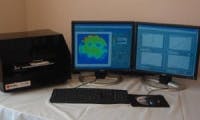
Date Announced: 15 Feb 2006 MaxMile Technologies, LLC at Lexington has released a series of electroluminescence (EL) mapping systems for the LED industry. These systems can be used to characterize the EL behavior of unprocessed light emitting wafers as a finished LED functions through electroluminescence. They are nondestructive in nature and can be used for wafer-level and micrometric-scale investigations. The systems may also be used to evaluate the photoluminescence (PL) and electrical properties of different regions in the light-emitting materials.MaxMile Technologies' EL mapping systems not only enable fast response for material development, but also its nondestructive nature will dramatically reduce the cost of quality control and improve cost-effectiveness. These EL systems will help the industry to accelerate the LED development and to overcome the hurdle to widespread market penetration. The EL systems can be widely used for:*fast response for light-emitting material development including recipe modification, growth and system optimization, *high-volume characterization ranging from wafer evaluation/screening to device sorting *LED research and development with the combined capability of EL and PL.
Contact
MaxMile Technologies, LLC Lexington, SC 29072, USA Tel: +1 803 996 0672 Email: [email protected]
E-mail:[email protected]
Web Site:http://www.maxmiletech.com/


