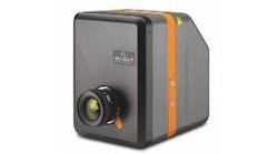
Date Announced: 14 Jul 2011 Portland, OR - ESI, Inc., a leading supplier of innovative laser-based manufacturing solutions for the microtechnology industry, today unveiled its most advanced LED wafer scribing system, the AccuScribe 2600. ESI's AccuScribe 2600 is built on patented, industry-leading technology enabling customers to extract the maximum light output from LED's. ESI developed the AccuScribe 2600 based on customer requirements for high brightness LED (HB-LED) manufacturing, including Patterned Sapphire Substrate (PSS), Distributed Bragg Reflector (DBR), Metal Mirror (MM) and other advanced light extraction technologies. The company is showcasing the AccuScribe 2600 this week at the SEMICON(R) West exhibition in San Francisco."ESI pioneered the laser scribing of LED wafers with our patented technology for LED sapphire substrates," said Jonathan Sabol, general manager of ESI's LED uEngineering Division. "Industry wide expansion of high brightness LEDs is driving rapid changes in LED architecture and manufacturing processes to continuously increase lumens/watt. The AccuScribe 2600 is specifically designed to match our customers' most demanding technology roadmaps while achieving industry best yield, performance and cost."Multiple customers have recently confirmed that the AccuScribe 2600 delivers the industry's highest brightness scribing for a wide range of HB-LED technologies including PSS and DBR metal mirror. Increased light output results in increased revenue and profitability for LED Manufacturers. This, coupled with achieving the highest yield, lowest cost, least environmental impact, and complete elimination of the employee work hazards related to chemical etching, will allow ESI Accuscribe 2600 customers to lead in the most profitable segment of the high brightness LED market.To learn more about ESI's AccuScribe 2600 and its full line of LED systems and applications, visit the company during SEMICON West at Booth #5871 in the North Hall at San Francisco's Moscone Convention Center. Editors interested in meeting with ESI during the show may contact Debbie Caldwell at 503-780-9695, [email protected] ESI, Inc.ESI is a leading supplier of innovative, laser-based manufacturing solutions for the microtechnology industry. Our systems enable precise structuring and testing of micron to submicron features in semiconductors, electronic devices, LEDs and other high-value components. We partner with our customers to make breakthrough technologies possible in the semiconductor, microelectronics and other emerging industries. Founded in 1944, ESI is headquartered in Portland, Ore., with global operations from the Pacific Northwest to the Pacific Rim. More information is available at www.esi.com .
Contact
ESI Debbie Caldwell 503-671-5405
E-mail:[email protected]
Web Site:www.esi.com