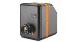
Date Announced: 07 Dec 2011 Montbonnot, France – Altatech Semiconductor S.A. has entered the light-emitting diode (LED) inspection market by introducing its new AltaSight LEDMax® system, the company’s first product designed specifically for detecting, classifying and characterizing defects on wafers used in manufacturing LEDs.AltaSight LEDMax improves production yields for LED devices by accurately detecting process-induced defects, including those that can result during metal-organic chemical vapor deposition (MOCVD) of epitaxial layers, subsequent patterning processes and final inspection. Using Altatech’s patented sensor technology that filters out all background noise, the non-contact system generates images of surface imperfections with resolution down to 1 micron and a unique depth-of-focus capability approaching 500 microns.An integrated review station performs real-time analysis of the gathered inspection data. It can stitch together images from different perspectives, generate 3D renderings and measure defect sizes. All defect-detection results are stored within the system, and can be output to an operator in standard file formats.“With its multi-class defect reporting and high accuracy, our newest inspection system meets the unique needs of LED manufacturers,” said Jean-Luc Delcarri, president of Altatech Semiconductor. “Altatech is entering this market by providing a defect-detection solution that traditional semiconductor-inspection tools cannot match in terms of reliability and cost-efficiency.”The highly flexible design enables AltaSight LEDMax to combine up to three inspection modules, allowing it to be used in volume manufacturing, process development or R&D applications.In addition to handling the full range of compound semiconductor wafers on which LEDs are produced today, AltaSight LEDMax has the versatility to meet other III-V inspection requirements. It can accommodate sapphire, silicon, silicon carbide and other transparent surface substrates. The system’s high flexibility and reliability extends to its ability to inspect thin and thick wafers as well as significantly bowed substrates. AltaSight LEDMax can handle four- to eight-inch wafers without any hardware changes, and a field-upgradeable option for handling two-inch substrates will be available in the coming months.Altatech has begun taking orders for AltaSight LEDMax from LED manufacturers around the world. Production units will be shipped to customers in the first quarter of 2012.About Altatech Semiconductor S.A.Incorporated in 2004, Altatech Semiconductor manufactures wafer inspection and analysis, liquid-vaporization CVD, and inkjet nanoprinting equipment at its headquarters facility near Grenoble and France’s epicenter of microelectronics production. Led by a management team with more than 30 years of experience in the semiconductor equipment industry, the company is focused on helping customers to achieve the fastest design-to-market cycle times for products serving the emerging semiconductor, MEMS and nanotechnology markets. For more information, visit www.altatech-sc.com.
Contact
Altatech Semiconductor S.A. Tel. +33 4 56 526 800 Bruce Hokanson 360-258-1260 [email protected]
E-mail:[email protected]
Web Site:www.altatech-sc.com


