This article was published in the September 2011 issue of LEDs Magazine.
View the Table of Contents and download the PDF file of the complete September 2011 issue.
+++++
Growing demand for high-brightness (HB) LEDs is prompting manufacturers to refine production methods and to develop devices with better performance. Achieving these ends requires precision metrology tools. In particular, critical metrology includes measurements of film thickness, and layer and substrate roughness, as well as detailed validation of patterned sapphire substrates (PSS).
This article describes two types of gauge-capable metrology tools that are currently used for these purposes: the atomic-force microscope (AFM), and the white-light interferometer (WLI). Because of its very high speed, the WLI in particular is poised to become a key quality-control (QC)/process-monitoring tool as production volumes of relatively new devices are pushed to ever higher levels. We compare and contrast these very different tools, showing where each is particularly well suited in the HB-LED life cycle of development through volume production.
PSS benefits
In conventional gallium nitride (GaN) on sapphire LEDs, total internal reflection – due to the large refractive-index difference between GaN and air – limits the amount of light that can be extracted from the device. Overcoming this limitation will enable HB-LED manufacturers to steadily increase two of the most important performance parameters – brightness and efficiency.
Final LED performance is strongly impacted by the quality of the substrate and the various layers. Key factors are the front- and back-side substrate wafer roughness, the roughness and uniformity of the various epitaxial layers, and the absence of defects in these epi layers, such as steps and pinholes. In the case of PSS, it is equally vital that the sapphire bumps are created with the correct dimensions (height and width) and the right pitch; testing protocols must ensure that malformed bumps or missing bumps are avoided.
AFM: the ultimate surface-metrology tool
The highest-resolution surface-metrology instrument available is the atomic-force microscope (AFM). It is now widely used by both wafer suppliers and LED manufacturers as a reference standard because it is capable of atomic resolution.
By raster-scanning the tip across the sample (or the sample under the tip), a quantitative topographic map of the surface can be created. The in-plane (or XY) resolution is mainly limited by the radius of the tip, and it is often 2 nanometers (nm), or sometimes even better. The resolution in the vertical (Z) dimension is not directly related to the tip, and is often better than 0.5 angstroms (0.05 nm).
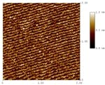
The AFM is also the definitive reference for the production of epitaxial layers. The XYZ metrology it provides is ideal for spotting film defects, such as steps and pinholes. It is also fast enough for measuring the roughness of these layers during new process development or modification, where its non-destructive nature is a significant advantage. And, once a process is proven, it is often the preferred tool for statistical sampling of final product.
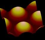
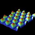
For R&D and some production applications, the AFM is still the preferred tool for PSS because it provides complete three-dimensional characterization of the critical surfaces, including slope, at atomic resolution if necessary. Indeed AFM manufacturers such as Bruker have developed dedicated AFMs for PSS applications (e.g. the Dimension Edge PSS). These tools combine the ability to automatically measure up to nine 2- to 6-inch wafers at a time with software that supports dual (engineering and operator) levels of access. This latter feature enables an engineer to set up measurement protocols as well as pass/fail criteria and then hand the tool off to a technician as a simple pass/fail diagnostic.
WLI supports high-volume PSS
For very-high production volumes, even AFMs designed specifically for PSS can be a testing bottleneck. The white-light interferometer (WLI) is a tool that better meets the needs of these applications. Specifically, the WLI can quantify the height, width and pitch of PSS features and readily spot defective features. In addition, it is an ideal tool for measuring surface roughness and the thickness of optically-transparent films that are greater than 1.5 µm in thickness.
The WLI, or optical profiler, is a non-contact, non-destructive tool that uses light waves as a high-resolution ruler or depth gauge. A WLI looks similar to a conventional optical microscope, and the device under test is placed on the sample stage. Light from a white-light source is sent into the objective, and is then split into two paths by a partially-reflective mirror. One of the paths is focused on the sample surface and the other is deflected to an extremely-flat internal reference surface. When these two reflections are recombined, the image contains a series of dark and light bands that are a direct function of the profile of the test surface; they are analogous to elevation contours on a topographic map. Moreover, they only appear as sharp stripes in the image where the microscope is perfectly focused on that part of the sample.
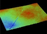
The WLI delivers extremely high dynamic range; that is, it provides vertical resolution of better than 0.1 nm over a range of feature heights up to 8 mm. In the (horizontal) XY plane, WLI image resolution depends on the choice of microscope objective. In addition to mapping the surface profile and features (Fig. 4), a high-performance WLI can also compute common statistical parameters such as RA roughness.
The WLI is already proving to be a robust tool for several different HB-LED metrology tasks including ITO (indium tin oxide) film roughness; GaN film thickness measurement; PSS pitch, width, height and uniformity; PSS defect inspection (non-valid peaks); and sapphire substrate top- and bottom-side flatness.
However, it is in the areas of profiling PSS wafer pitch, width and height, as well as defect inspection, that the WLI’s speed is proving to be a critical advantage.
The optimum WLI magnification for PSS work appears to be about 230×, which delivers the best combination of field of view (i.e. speed) with the XY resolution required for pass/fail operation and process feedback. For example, the 20 micron2 field-of-view per measurement enables 13 such sites to be analyzed per 2-inch wafer in just 2 minutes. This corresponds to more than 60 wafers per hour.
Depending on the HB-LED specifics, a 20 micron2 field-of-view corresponds to between 20 and 100 PSS features. Moreover, the standard deviation of measured height is less than 6 nm (3σ, and less than 10 nm (3σ) for width. The use of automated internal calibration means excellent gauge capability; the 3σ standard deviation of height, width, and pitch is less than 10 nm over a five-day period.
Conclusion
For conventional LEDs, the AFM remains the ultimate surface-metrology tool for LED fabricators and wafer vendors alike. It’s also an ideal solution for development and qualification of new production processes, such as for PSS HB-LEDs. But when these HB-LEDs go to very-high-volume production, dense sampling can often be better served by a WLI. This is a versatile tool that is also useful for other HB-LED QC/metrology tasks including surface roughness and gauging thickness of optically-transparent films.


