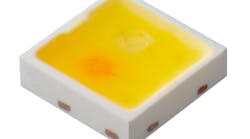
LED-based solid-state lighting (SSL) systems are commonplace in all kinds of electronics, from smartphones to camera flashes and car headlights to home lighting. According to the US Department of Energy (DOE), last year nearly 13% of new lighting installations both inside and outside buildings were LEDs, up from 3% two years prior. LED technology is seen as state of the art as far as lighting systems go and represents a significant opportunity for design engineers.
Because LED lighting is based on solid-state technology, it has several advantages and drawbacks. The principle advantages include reliability, longevity, performance, and energy savings. LEDs have an expected lifetime (≥80% of initial luminance) of 5 years or 50,000 hours of continued use. This performance parameter is known as lumen maintenance, with LM-80 being the familiar IES (Illuminating Engineering Society) method for measuring lumen depreciation and TM-21 the technical memorandum that describes how to use the data to project long-term performance. Because they are based on solid-state technology, LEDs do not “burn out” as do incandescent bulbs and are therefore more reliable than their counterparts. In addition, they make a significantly larger contribution toward energy savings than other lighting systems.
Notwithstanding these advantages, LEDs have three major drawbacks. Like all semiconductors, they are sensitive to electrostatic discharges (ESD) events. They are also susceptible to overvoltage spikes. Third, they require overtemperature protection.
Preventing ESD in LEDs
For these reasons — and primarily due to ESD — discrete protective components have traditionally been used to protect LED lighting systems, depending on the series and parallel connection of the individual LEDs. Transient-voltage-suppression (TVS) diodes provide such protection by offering a low-voltage clamping capability, ensuring that the voltage remains low. Without a TVS diode, there would be a sudden spike of voltage that could cause failure in the SSL system. In conventional LED lights, the TVS diode as an ESD protective component is positioned next to the LED on the substrate (Fig. 1).
Within the last decade, an alternative has arisen in the form of multilayer varistors. Not only are they compact and inexpensive, but multilayer varistors are better at protecting LEDs against ESD. These are surface-mount device (SMD) components that can withstand temperatures up to 125°C without derating and thus exhibit significantly better temperature derating than TVS diodes. Moreover, multilayer varistors enable the use of a single soldering process for mounting instead of complex wire bonding on printed circuit boards (PCBs).
Combine protection with substrates
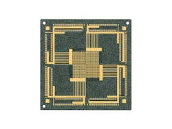
Now a third alternative has been developed: An ultrathin ceramic substrate, explicitly designed for LED systems, called CeraPad features a multilayer structure that provides integrated ESD protection and eliminates the need for discrete ESD protectioncomponents.
This approach offers a more efficient utilization of the PCB surface by the light source than using discrete components and multilayer varistors. As a result, the protection component does not interfere with the optimum radiation of the light produced by the LED, allowing for a higher LED efficacy. The ceramic substrate can be customized for application requirements and supplied to a customer for PCBimplementation.
Eliminating the additional discrete ESD components further increases the LED mounting density (Fig. 2). This results in cost savings, more efficient use of the substrate surface, and improved reliability. In addition, the elimination of TVS diodes and bond wires — and therefore associated cost-intensive component placement and process steps — increases manufacturing efficiency, quality, and the overall robustness of the component. While not meant to be a direct comparison of TVS diodes, the strength of ESD capabilities is one reason why the technology is superior to silicon-based Zener diodes for LED applications. It is also one reason why this type of TVS diode is most often used for LEDprotection.
FIG. 2. Shown is the design of an LED unit where the ESD protection is embedded directly into the substrate below the LED. Chip-scale packaging (CPS) permits a high packing density.
The functional CeraPad wafer provides a stable LED substrate with an ESD strength of up to 30 kV. This is more than three times higher than that of Zener diodes, which only offer 8 kV. CeraPad also enables customized chip-scale packages (CSPs) to be implemented for standard LED elements from CSP0707 to CSP1515 with a considerably higher packing density. Furthermore, CeraPad offers a low coefficient of thermal expansion of 6 ppm/K, which is nearly identical to that of silicon-based LEDs, meaning that no additional thermal protection is required.
With this technology, there is little mechanical stress between substrate and LED when the temperature changes, as the ceramic substrate features a high thermal conductivity that can be further increased by means of silver thermal vias. In the case of the CeraPad, there is a high bending strength of 250 MPa for a substrate thickness of just 300–400 µm. There is low coefficient of thermal expansion, high thermal conductivity, and high bending strength, which combine to make customizable CSPs viable.
Applications
By combining multilayer ESD protection components and low-temperature co-fired ceramic (LTCC) substrates, the technology can also be used as a redistribution layer, similar to a conventional PCB. Testing has shown that as many as ten such redistribution layers can be implemented in this way without compromising the thermal performance. This stands in contrast to the use of a conventional isolated metal substrate (IMS) where thermal conductivity decreases with each additional layer, and only five redistribution layers can reasonably be implemented before thermal performance is compromised.
In the case of the CeraPad substrate, it is possible to place as many as 1000 tightly packed LEDs on the substrate, which are individually controllable. Due to the nature of the design, there are no additional driver needs to take care of potential power surges as power protection is built into the substrate.
With this technology, engineers can create high-resolution lighting in space-constrained applications. Such examples may include multiple LED flashes in smartphones, automotive interior lighting systems, or in adaptive vehicle headlights. The level of ESD protection delivered by the ceramic substrate helps product developers better meet quality standards and increase the lifespan particularly in such compact designs.
In the case of automotive headlights, the ceramic substrate technology gives automakers the ability to have individual control over each LED within the headlight matrix that allows it to be adaptive to its environment and other programmed signals. As an example, the engineer can design the headlight to dim the light level automatically when both oncoming traffic is approaching and the car is turning a corner. Additional LED pattern control allows for lights to brighten when there are no other automobile headlights approaching.
FIG. 3. The CeraPad design shown provides a 16×16 LED array consisting of CSP0707 LEDs. With some customization, it is possible to place as many as 1000 tightly packed LEDs, which are individually controllable.
Conclusion
While the costs would not be good for retrofit or repair applications, any increased costs are typically overcome by long-term cost savings over the life of the component. Due to the ability to highly customize the CeraPad design, the cost varies for every implementation depending on the layers and number of LEDs used in theapplication.
Combined multilayer ESD protection components and LTCC substrates help engineers meet the technological challenges of increasing sensitivity of integrated circuits and continue to drive the miniaturization of LED modules. This will allow for innovative and optimized SSL designs with increased light yield from LEDs.
SONJA BROWN is senior product manager – Piezo and Protection Devices at TDK Electronics Inc. (www.tdk-electronics.tdk.com).


