Government-funded group targets 2020 for prototypes using aluminum gallium nitride.
Osram Opto Semiconductors said it is leading a government backed consortium to develop what Osram described as a high-power, mass-market ultraviolet (UV) LED chip.
Interested in articles & announcements on UV LED technology in specialty SSL applications?
Ultraviolet light is used in a wide variety of applications such as curing (drying), disinfection, production, medicine, and the life sciences. Conventional non-LED sources such as mercury vapor lamps come with certain potential hazards. And many of the UV LED chips already on the market don’t yet economically emit at certain useful wavelengths, although we recently reported on a UV LED breakthrough announced by LG Innotek.
“The partners have made it their goal to provide high-power UV LEDs to cover a wide variety of applications,” Osram said. “These LEDs will eventually replace conventional UV light sources, which often contain toxic mercury.”
Osram said the new high-power chips “are also likely to open up new areas of application.”
UV is an emerging field for LED makers. Suppliers include RayVio, Nikkiso, Vital Vio, Sensor Electronic Technology, and the aforementioned LG Innotek, among others.
The Osram-led consortium is funded by the German Federal Ministry of Education and Research (BMBF). It hopes to develop a prototype by 2020 operating from around the 250-nm wavelength to around 310 nm, which spans parts of the UV-B and UV-C spectrums.
Ultraviolet light in general runs from around 100 nm to around 380 or 400 nm. It is the short-wavelength invisible portion of the spectrum that eventually gives way to longer-wavelength, lower-frequency visible light starting with violet.
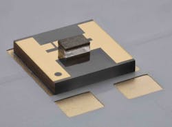
Osram released this photo of a UV LED chip under development, from the Ferdinand-Braun-Institut, Leibniz-Institut fur Hochstfrequenztechnik (FBH).
One of the challenges has been to improve efficacy in the UV-B and UV-C spectra, which requires advances in materials, and which extends applications beyond UV-A’s curing usefulness. The Osram-led group is working with an aluminum gallium nitride (AlGaN) material system.
In addition to Munich-based Osram, the four other research groups are: the Ferdinand-Braun-Institut, Leibniz-Institut fur Hochstfrequenztechnik (FBH); the Technical University of Berlin; LayTec AG; and UVphototonics NT GmbH, a spin-off of FBH.
Osram is responsible for the 270–290-nm range. FBH is handling the epitaxy in the 290–310-nm range and processing the epitaxial wafers into UV chips. The Technical University of Berlin brings expertise in AlGaN and is focusing on the 250–270-nm range. LayTec is contributing techniques for controlling the epitaxy and plasma etching systems, and FBH is optimizing the chip design, with an eye on high currents and efficient cooling. It is also collecting process data from the other partners and making it available to the consortium.
“The optical outputs of the new LEDs are expected to be greater than 120 mW at 300 ± 10 nm, 140 mW at 280 ± 10 nm and 80 mW at 260 ± 10 nm,” Osram said. “The research group is also working on making significant improvements to the aging behavior of the LEDs so they can be operated longer and more economically.”
MARK HALPER is a contributing editor for LEDs Magazine, and an energy, technology, and business journalist ([email protected]).


