This article was published in the February 2012 issue of LEDs Magazine.
View the Table of Contents and download the PDF file of the complete February 2012 issue.
+++++
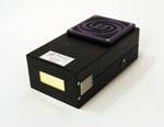
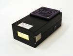
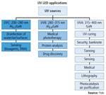
Below the visible spectrum lies a band of wavelengths called ultraviolet (UV). Ranging from 100 to 400 nm, the radiation can effectively be used to sterilize cosmetics, perform forensic analysis, cure materials (Fig. 1) and disinfect water, among many other applications. Today, as is the case with LEDs in the visible spectrum, UV LEDs are only beginning to replace the established UV sources in a likewise diverse array of markets.
By far, the UV curing market is enjoying the greatest surge in UV-LED adoption due to the relatively recent breakthrough in flux density of UV-LED chips beyond the 4W/cm2 mark at the different wavelengths needed to bring UV-LED curing into production facilities. “For the first time, LEDs have reached the power densities that make UV LEDs competitive with existing sources,” said Uwe Thomas, general manager of emitter components with LED Engin, a provider of UV and visible LEDs based in Santa Clara, CA.
UV-A, B and C
Curing involves the cross-polymerization of a photosensitive material, which can be an ink (printing), adhesive or coating, and is primarily performed at 395 nm, 385 nm or 365 nm, wavelengths which are part of the UV-A spectrum (315-400 nm). Another important UV-A application is inspection systems based on machine vision. UV-LED flashlights in this range are used to detect fraudulent identification and currency, and offer the benefit of use in well-lit environments, which is difficult using a mercury-vapor lamp.
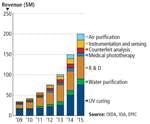
In the UV-B spectrum (280-315 nm), applications for UV LEDs include curing, medical light therapy, forensic analysis and drug discovery. It has been estimated by market research firm Yole Développement (Lyon, France) that 90% of UV LED applications today are based in the UV-A and UV-B regions (Fig. 4). Yole has stated that it expects the market for UV LEDs to grow by 30% annually from $25 million in 2010 to more than $100 million in 2016. Fig. 5 shows an even more optimistic forecast from the Optoelectronics Industry Development Association, the International Optoelectronics Association and the European Photonics Industry Consortium.
In the lower UV-C spectral range (100-280 nm), the primary LED applications are air and water sterilization and a range of analytical tools including those that perform spectroscopic and fluorescence measurements. Chemical and biological detectors also work in this spectral range.
UV in the 250-275 nm range sterilizes water, air and surfaces by breaking-up the DNA and RNA of microorganisms and preventing their reproduction. Specifically, 275 nm is believed to be the most effective wavelength for eradicating pathogens such as E-coli in water. In fact, engineers at Sensor Electronic Technology Inc. (SETi), based in Columbia, SC, have determined that 275 nm is the optimum wavelength for water disinfection. SETi has demonstrated disinfection of drinking water in an in-line flow-through system using less than 40 mW of UV power.
Alternatives to mercury arc lamps
In production curing operations, mercury-vapor lamps are hindered by short lifetime (2000-10,000 hr), slow warm-up and cool-down times, and wide spectral power distribution. “In addition, over 60% of the energy that is applied to a typical mercury-vapor lamp is radiated back out as infrared energy, in other words, heat,” said Eskow. He added that the UV output of a mercury vapor lamp drops off rapidly over its operational life because some of its electrode material vaporizes, depositing a film on the inside of the quartz tube which the UV cannot penetrate. As a result, the user cannot easily predict the amount of UV generated at a later time; often this is a critical process parameter.
Metcalf added that many people who would not have considered UV curing because of the complexity of standard curing processes – the high voltage, heat of mercury bulbs and environmental issues – will now consider UV-LED curing because it subverts the traditional hassles of the old process.
UV LEDs bring such benefits as knowing precisely what power level is being delivered to the curing medium, as well as other advantages LEDs are known for, such as the ability to pulse-width-modulate the output, stated Eskow.
The transition to UV LEDs also opened the door to more environmentally friendly curing formulations. With the next generation of products that ink, coating and adhesive companies were developing, they used the opportunity to phase-out volatile organic compounds (VOCs) associated with the solvent-based formulations of past chemistries.
Curing optimization
For the longer-wavelength UV devices, in a similar manner to blue LED fabrication, InGaN-based epilayers are grown on sapphire substrates to produce 385, 395 and 405 nm UV LEDs for curing. One key advantage to higher-wavelength devices is that they can be driven at higher power. “395 nm is really the sweet spot for UV LED curing, because at 405 nm the formulation is sensitive to ambient light, so you want to be just below 400 while being able to drive the LEDs at high power,” said Lim. All the major providers of curing formulations (photoinitiators and resins), have recently brought higher-wavelength inks and coatings to market to fill this need.
Curing processes require large, high-power LEDs (multiple die/chip) arranged in a tight matrix in a chip-on-board configuration, close to the emitter window with either an air- or water-cooled internal system to remove heat from the backside of the board. “It doesn’t matter what the UV intensity is at the emitter window, what matters is the intensity at the surface of the media,” said Metcalf. Depending on the equipment and curing application, the media can be 1 to 100 mm from the emitter window, for which AMS has produced special optics. In addition, a metal-cooled PCB is used to sink the heat away from the matrix of LEDs.
Air cooling is also used. For instance, the curing system shown in Fig. 1, which has an emitter window of 150 x 20 mm and flux density of 4W/cm², can be used for spot curing inks, coatings or adhesives. Today, UV-LED curing equipment is often specially designed to fit the application. Metcalf describes large flat-bed banner printers as being able to use lower-power LEDs, but higher speed digital, offset and flexographic technologies require closely-spaced banks of high-flux-density LEDs. Even though the radiation is not visible, collimating optics are utilized to deliver the radiation with a uniform power level across the target media. Digital inkjet curing was the first segment to adopt UV LEDs due to the required close distance to the media for the print heads to optimally perform. This was a natural fit for UV-LED lamps as the curing intensity is highest at the emitter window.
One of the issues the curing industry has faced has been inconsistencies in measurement practice and parameter definitions, for example, defining radiometric intensity. The UV LED Curing Association (www.uvledcuring.org) has been formed recently by curing manufacturers Phoseon Technology, Integration Technology Limited and Lumen Dynamics to “set guidelines and ensure compatibility across the industry,” stated Bill Cortelyou, President and CEO of Phoseon Technology. The association also seeks to help speed development of applications especially suited to UV LEDs, educate researchers, integrators and end users regarding the benefits of UV LEDs, and provide a forum for industry communication and collaboration.
“In our 15 years of experience in LED curing technology, the industry has realized significant breakthroughs that have proven LEDs as a viable alternative that provides substantial benefits,” said Allan Firhoj, President and CEO of Lumen Dynamics based in Ontario, Canada. He added, “The UV LED Curing Association will be instrumental in helping the market gain knowledge and insight about UV LED technology and its numerous commercial benefits.”
A second association, the International LED-UV Association (www.leduv.org), was formed in September 2011 in Japan to organize makers of UV-LED printers, UV-LED manufacturers and ink and coating formulators that are committed to developing sustainable and the environmentally friendly UV-LED printing technologies.
Chip manufacturers
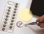
Companies that manufacture UV-LED chips include Crystal IS, based in Green Island, NY (Fig. 3); Dowa Electronic Materials Co. Ltd., based in Tokyo, Japan; Nichia Corp., based in Tokushima, Japan; SemiLEDs, based in Hsinchu, Taiwan; SETi, and Seoul Optodevice Co. Ltd., based in Kyunggi-do, Korea, a wholly-owned subsidiary of Seoul Semiconductor.
Tim Bettles, director of marketing and sales at SETi stated that its manufacturing agreement with Seoul Optodevice is designed to help SETi drive its volumes of UV LEDs and lamps higher while driving down costs. “Our first UV-LED products were launched in 2004 and since then, we have come a long way in both technology development and market adoption. We are now gearing SETi’s capacity for high-volume manufacturing to cater to new demands coming from mainstream consumer markets,” said Bettles. SETi recently announced the purchase of a new facility, where it plans to manufacture over 100 million UV LEDs per year.
Devin Tang, marketing manager of SemiLEDs stated that the company has a full line of bare dice and surface-mount high power packaged LEDs in the 360-400-nm range. He noted that the company’s products are differentiated from others with respect to the chips’ copper-alloy substrates, which allow high thermal conductivity (400 W/mK) and silicon substrates in the packages, which reduce cost.
Epigap Optronic, based in Berlin, Germany, the main distributor for Dowa’s UV LEDs, stated that Dowa manufactures 265, 280, 310, 325 and 340 nm bare dice or packaged LEDs. Nichia manufactures 365, 375 and 385 nm surface-mount high-power LEDs and low-power lamps. Crystal IS manufactures 260 nm UV LEDs and is the only company to produce LEDs on AlN substrates.
Wafer-processing issues
As was indicated previously, epilayers of InGaN and GaN, grown by MOCVD, are used for higher-wavelength UV LEDs fabricated on sapphire substrates, but at lower wavelengths, epilayers of AlGaN with increasing aluminum content must be used. There are many different compositions involving layers of AlGaN, AlInGaN, AlInN and AlN epilayers, but whatever the composition, it becomes easier to grow AlGaN-based materials on AlN substrates than sapphire at some point, which has encouraged the development of AlN-substrate suppliers such as Hexatech, based in Morrosville, NC. Nonetheless, AlN substrates are only available in small sizes and remain much more expensive than sapphire wafers, thereby limiting this market.
Optics and packaging
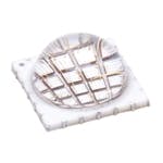
Even though UV LED manufacturers have been working hard to improve internal quantum efficiency and optical efficiency, overall efficiency remains below 20%, meaning a great deal of heat must be dissipated from the diode’s junction. “To achieve the required flux densities with today’s chip technologies, the multi-die emitters need to be driven at the highest current. This is only possible with an LED package capable of handling extreme power densities for the life of the product. A thermally matched stress-free package and glass lens help eliminate common packaging failure modes associated with UV LEDs,” said Thomas. He described LED Engin’s patented multi-layer ceramic substrate with extremely low thermal resistance that quickly conducts heat from the die junction (Fig. 2).
While some UV LED arrays are packaged on ceramic substrates, many manufacturers, particularly of single-chip devices, use TO-can type through-hole packages with a glass top that offers high transmission of UV. The replacement of epoxy lenses with flat or dome-shaped glass capable of UV transmission is a relatively new development, and one that has allowed an extension of lifetimes from around 5000 hours up to as high as 30,000 hours. UV accelerates degradation of the epoxy material in a non-linear manner, directly impacting lifetime. The glass lenses provide enhanced durability and improved reliability. Another alternative is to combine a glass lens with silicone encapsulant to accommodate even higher flux density and higher efficiency yet shorter lifetime (15,000-20,000 hr).
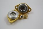
The choice of whether to use hermetic sealing in the package is sometimes determined by the materials in the chip. “An aluminum-nitride substrate almost dictates the use of a hermetic package, because the higher the aluminum content, the higher the device's affinity for oxygen, so a hermetic seal will protect the UV device better,” explained Frank Gindele, product development manager for Schott Electronic Packaging in Landshut, Germany. The new copper- and glass-based package from Schott offers the advantages of high thermal conductivity and hermeticity.
Dangers of UV
It is important to recognize that some of the same qualities that make UV LEDs very powerful and useful – their low wavelength and high energy – are also the qualities that make them dangerous. The warning labels on UV LEDs and their products are clear but bear noting: UV-LEDs emit invisible ultraviolet radiation when in operation, which may be harmful to eyes or skin, even for brief periods. (For more information on photobiological safety, see our series of articles, Part 3 of which appears on p.63 of this issue.)
Next steps
When asked to identify the key issue that might keep UV users from changing over from mercury-vapor sources to UV LEDs, many industry participants say it comes down to breaking existing industry momentum and, of course, cost. Lim thinks that a rounding out of the wavelength portfolio would go a long way toward adoption. “I think if we can get good 250-nm, 285-nm and 300-nm LEDs, those three wavelengths, then we can pretty much shut the door on mercury arc lamps.”
