This article was published in the February 2013 issue of LEDs Magazine.
View the Table of Contents and download the PDF file of the complete February 2013 issue, or view the E-zine version in your browser.
+++++
In the search to cut the costs of manufacturing LEDs, switching to large diameter (6-8-in, 150-200-mm) substrates is often brought up as a key solution. In fact, it is mentioned so often that one might assume a mass transition to large diameter has already occurred. Such a transition has been slow to happen due to both technical and logistical challenges. But as we will discuss, the advantages will ultimately be significant enough that the LED manufacturers will move to larger substrates, reduce component costs, and further accelerate the adoption of solid-state lighting (SSL).
This may come as a surprise because the demand for large diameter should be very high – it has often been cited as a fundamental cost saver to drive down LED chip prices. With the industry-wide search to drive down cost significantly, and large diameter seen as a key way to accomplish this, why aren’t more chip producers making this switch?
To answer this question, we will look at three areas. First, what are the true benefits of large diameter? Second, if the benefits are truly great, then why aren’t more manufacturers switching? Finally, we’ll look at some of the potential disruptions that might bring quicker large diameter adoption, such as c-axis CHES (controlled heat extraction system) technology – along with the prospect of 8-inch substrates.
More LED chips
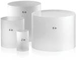
We’ll begin by looking at the main advantage of moving to larger wafers – more LED chips. Yes, this is the biggest advantage, but it’s also unfortunately often overstated in this way: a large diameter 6-in wafer has nine times more surface area than a 2-in wafer on which to form LED chips (Fig. 1).
While the prior statement is certainly true in regards to the simple surface area of the wafers, the suggestion that you get 9× more chip throughput by simply using 6-in wafers sounds too good to be true – and it is. What’s the real story? In order to answer that, we need to look closely at the layout of LED chips, both on the wafer and as a group of wafers in the MOCVD (metal organic chemical vapor deposition) reactor where LEDs are formed.
In addition to 6- or 8-in wafers simply being larger, we have to consider several other factors to get a true picture of the benefit of “more LED chips.” These factors are exclusion zone, LED chip shape and size, and MOCVD reactor layout. We’ll explain these one at a time, then feed them into a true comparison simulator that will give us a much more reasonable look at the number of LED chips supported by various wafer sizes.
Exclusion zone
We will first look at what’s called the exclusion zone on a wafer. During epitaxy, LED material is not properly formed in this area, meaning these chips shouldn’t be counted because they will not result in good LEDs. For our LED chip calculator, we are using an industry standard 3-mm exclusion zone, which is shown as red chips in Fig. 2. Note that the chips on the extreme edge of the wafer – that are actually hanging off the wafer if they were full rectangles – are not going to be counted at all for our simulation.
One important characteristic of the exclusion zone is that it is 3-mm from the edge regardless of wafer diameter. This fact means that the large diameter wafers have larger exclusion zone areas. However, as a percentage of the total wafer surface area, the large wafers have a smaller proportion of their area in exclusion zones.
So you can see how a 6-in wafer that has 9× more gross surface area actually has more than 9× more net area (gross area minus exclusion zone). The advantage results in 6-in wafers having 10.3× more net area, and 8-in wafers having 18.8× more, both as compared to a 2-in wafer.
MOCVD reactor layout
At this point, we’ve seen that a 6-in-diameter wafer actually holds slightly more than the often-quoted 9× more LED chips compared to a 2-in wafer. But now we have to consider that LEDs are grown in groups of wafers in an MOCVD reactor.
The LED epitaxy process is one of the most expensive and time consuming of all the steps that go into the final delivery of an SSL product. The input is a group of wafers, and the output is thousands of LEDs on those wafers. What we are seeking to answer is how switching to large diameter will change that LED count after the epitaxy process. Of course, yield – a measure of chips that function correctly – matters too, but we will look at that later.
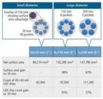
We’ve already said that you shouldn’t expect the chip count you get after epitaxy to jump by a factor of nine, and now we’ll see why. The primary reason is the fact that so many more small-diameter wafers can fit in the reactor chamber. In a typical MOCVD reactor configuration, 56 2-in wafers can be loaded. In the same reactor only eight 6-in wafers will fit. That’s a ratio of 7:1 in favor of small diameter.
So to simply break even in the final count, each 6-in wafer would need to hold 7× more LED chips than a single 2-in wafer. However, we’ve already seen that a 6-in wafer has almost 11× more LED chips. Put in other terms, the 6-in configuration results in 55% more LED chips (1.55×). This is the final true advantage we’ve been looking for. While this is much less than the 9× (900%) figure that we started with, it is still a very significant improvement in the number of LED chips you get for the same cost of time and money for an MOCVD run. You can compare a typical MOCVD layout for small and large diameter wafers and their respective chip counts in Fig. 4.
LED chip size
We do need to consider another factor, and that is LED chip size. For our calculations we’ve used 45×45-mil rectangles, including the street width, or spaces between the chips. This size – around one square millimeter – is typical for high-brightness LEDs and is therefore a good comparison. However, as chip sizes increase the advantage for large diameter wafers also increases slightly. For example, if you use a 60×60-mil rectangle, the advantage for 6-in wafers increases to 58%.
For 8-in substrates, the advantage is a very large – 77% more LED chips over 2-in – and that is only from the five 8-in wafers that can fit in a typical MOCVD reactor. Comparing a move from 6-inch to 8-in directly, there is a 14% gain.
We now have an accurate view of the advantage large diameter brings to the LED chip count: 55% more for 6-in and 77% for 8-in. While these are impressive numbers, one factor we haven’t taken into account in our LED chip simulation is LED chip yield. We will look at this important factor next.
Higher yield
Each step in the manufacturing process of an LED chip has a yield loss, from the preparation of substrates through chip packaging. The yield losses at each step add up and contribute to a significant portion of the final chip cost. There is therefore a great deal of focus currently on improving yield in all of these areas.
Switching to large-diameter LED manufacturing has been linked to yield improvement in a number of stages of the manufacturing process. The potential benefits come both directly as the larger wafer size is a more uniform surface for epitaxy and indirectly through the use of better manufacturing equipment and techniques. While yield can be a complex subject, we will briefly look at some highlights of the possible benefits.
The second component of improved yield comes from access to modern process control and automation tools, which are designed around large-diameter wafers and have been perfected in IC manufacturing. Today’s commonly used small-diameter manufacturing techniques use manual processes, requiring many human interactions, and lack sophisticated tracking that could spot yield issues. Many experts have pointed to a general need to move from a research-style production environment to a true mass production environment. Let’s look in a little more detail at what this means.
Automation primarily refers to the use of machines to handle and transport wafers – removing the human element. Wafers can be moved faster and with less damage through automated machines instead of being hand carried. The benefit is a combination of fewer skilled operators required, less loss of wafers due to mishandling, and quicker movement through the manufacturing steps.
In addition to more automation, the use of more modern tools brings better process control. Process control is the use of data analysis to detect and predict problems that cause yield losses in any area of the production process. This involves a tracking and analysis of the substrate throughout the process, extending back to the crystal growth stage. Process control also takes into account the analysis data recorded by the various production tools.
The use of process control is often cited as a necessary step in advancing the LED industry. As with automation, the tools needed for implementing process control are designed around large-diameter substrates, so the benefit to switching goes beyond just more LED chips. For additional information on the industry’s move to improve yield through large-diameter wafer production, see the article “LED wafer and automation standards are on the fast track, ready for more industry feedback” (www.ledsmagazine.com/features/8/10/9).
Market conditions
At this point, we’ve seen how switching to large diameter wafers can create more chips per MOCVD run and improve yield in several areas. Yet the industry this year is still predicted to produce over 80% of the LED capacity using small-diameter substrates. Why? The reasons come from two factors: difficult market conditions and technological challenges in supplying large diameter substrates at a competitive cost.
Technology barriers
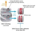
The second barrier to the adoption of large diameter substrates is a group of technological hurdles. It begins with challenges in sapphire crystal growth – the first step in creating substrates. As you can see in Fig. 5, today’s sapphire for HB-LEDs is typically grown on the a-axis, even though HB-LEDs require c-axis wafers. To get c-axis wafers from a-axis sapphire boules, a core must be taken sideways – wasting a large part of the sapphire.
Today’s a-axis sapphire growth technologies also result in defects that cannot be avoided when coring for large diameter applications. The volume of a 6- or 8-in core is so large that the defects become unavoidable and the cores must be shortened or scrapped. The total losses from sideways coring and defects waste over 80% of the material. For 8-in applications, the waste is over 90% and the production costs double.
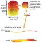
Another barrier caused by a-axis growth is that the resulting wafers have a variation in stress and strain across their surface. Because the wafer is from a sideways core of the boule, and the boule is grown along the a-axis, the wafer itself has a long growth time signature across its surface. This becomes significant during epitaxial growth when the wafer is heated.
The last technology barrier is in the slicing and polishing of the wafer and application of PSS techniques. Slicing and polishing are difficult processes and must be done well to generate good yield during epitaxy. Because the large wafers are 9-16× larger, the difficulty increases significantly.
PSS application faces a similar challenge, with the additional obstacle that the pattern can only be seamlessly applied to a limited size area smaller than 6 in. In order to get PSS on a 6-in wafer, a stepper (a semiconductor manufacturing tool) must apply multiple patterns, which is common in the silicon industry. However, for HB-LEDs the edges of the multiple pattern applications must be closely matched or LED yield will drop. This accuracy requirement is proving to be very challenging.
These barriers of market conditions and technology challenges have created multiple limitations for the mass adoption of large-diameter substrates. In the future, the market demand will require the throughput and yield only available using larger substrates, and as a result the technology challenges will be overcome. As proof of the possibility of overcoming the challenges, several tier-1 manufacturers have already made the switch and are positioned with an advantage over the majority of the industry.
Potential substrate disruptions
It is certain that HB-LED manufacturing will ultimately move to large-diameter substrates. The question is how quickly, and what material will be used for the substrates? In this last section we’ll briefly look at potential answers to these questions.
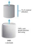
The main challenges we noted were the low material utilization due to a-axis growth and the high level of defects that make larger wafers expensive. There are alternative growth technologies that can grow directly on the c-axis for much lower waste. In addition, growth technologies that avoid significant defects are also available.
Sapphire grown with these characteristics of c-axis growth (also called on-axis growth for LED applications) and low defect levels are very well optimized for large-diameter applications. As you can see in Fig. 7 depicting c-axis CHES technology, the problems of low material utilization and high defect levels are both solved at once, with the additional benefit of a near net shape boule. The result is over 75% utilization for both 6- and 8-in applications.
In addition, the problems of warp during epitaxy that we saw from a-axis-grown sapphire are reduced as the c-axis CHES wafers are grown with a single time signature across their surface (Fig. 8). Because of these advantages, it is expected that as more manufacturers move to large-diameter applications, the growth technologies will also transition to c-axis, low-defect-level growth.
Because LEDs have such a broad potential market, there will be room for these alternative substrates along with sapphire remaining predominant. For example, an advantage GaN substrate brings is higher performance per chip – albeit at very high cost. This substrate may find a niche where a single bright LED chip is desired or required.
The next diameter past 6-in is the 8-in wafer. These wafers give another dramatic gain in LED chip count and further opportunities for yield improvement. Yet the barriers we examined earlier are the same, with the addition of the sapphire substrate costs doubling over 6-in using a-axis growth methods. Therefore the prediction is that one of these alternative technologies (sapphire grown on c-axis, silicon, or another substrate) will become dominant for 8-in wafers and beyond.
Obstacles and benefits
In summary, we found a move to large-diameter-based LED manufacturing provides a 55% increase in LED chips per MOCVD run using 6-in wafers, and a 77% using 8-in wafers. In addition to more chips, the yield would increase throughout the manufacturing process due to better epitaxy yield, automation, and process control.
The reason these advantages haven’t become common except with the largest LED manufacturers are several market and technology barriers. These include a-axis sapphire growth technology, a depressed market, and the use of PSS. But new c-axis-growth technology provides an optimized path to supplying large-diameter sapphire substrates. Other substrate materials, such as silicon, will likely find niche uses with some manufacturers. The advances of larger wafers will continue to the next step of 8-in.
Large diameter has already been proven by large tier-1 manufacturers as an important component in reducing costs and increasing performance of HB-LEDs. See “Philips Lumileds announces workhorse Luxeon T LED family” (www.ledsmagazine.com/news/9/12/7) for an example.
Yet many companies are staying with small diameter wafers until the next demand wave comes. However, companies that are planning ahead to gain a competitive edge – as is possible with large-diameter LED manufacturing – will be more efficient, more flexible to meet demand, and find success in the future.
