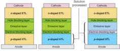
The typical layer sequence of an OLED using Novaled’s PIN structure—a p-i-n sandwich of a p-doped layer, an insulator, and an n-doped layer—starts at the bottom with an inorganic anode that is usually made from indium tin oxide, or ITO (see Fig. 1). The organic layer stack consists of a doped hole-transport layer (HTL), blocking layers around the central light-emitting layer, and is finished by a doped electron-transport layer (ETL). The cathode is typically made from an inorganic material such as silver.
Redox (reduction-oxidation) doping of organic transport layers with molecular dopants offers several advantages including low driving voltages, wide choice of materials for cathode and anode, and good power efficiency.1 Novaled’s redox doping transport materials have long been used successfully for OLEDs in which all layers were deposited using vapor thermal evaporation (VTE). Recently, we investigated OLEDs in which some layers were deposited using solution processing. These hybrid OLEDs fall into two main categories: OLEDs in which only one layer is deposited by solution processing and the subsequent OLED stack is deposited in vacuum, and OLEDs that have multiple solution-processed layers with only the final layer stack deposited in vacuum. Both approaches have specific advantages and challenges.


