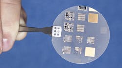
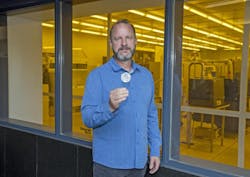
Long used as an electrical insulator, aluminum nitride (AlN) might be a key to unlocking newfound capabilities for LEDs, high-power electronics, and optoelectronics — but as a semiconductor. The high thermal conductivity and electrical insulating abilities of the material, an engineered ceramic, suit its current use in electronic devices for heat dissipation. Recently, a Georgia Tech research team led by computer engineering professor Alan Doolittle has found a way to create an ultrawide bandgap (UWBG) semiconductor with AlN that can be used at significantly higher power and temperature levels than previously achieved — and at more than five times the voltage of existing wide bandgap semiconductors, according to Doolittle in a Georgia Tech article. The enhanced robustness of UWBG semiconductors mean that fewer semiconductor devices are needed in high-voltage circuits, increasing performance and efficiency.
A bandgap is the minimum energy required to excite an electron into a state of conduction, for electricity to flow within a material; the bandgap also relates to wavelength of the light produced by the material and affects the breakdown voltage at which a device fails, according to the Georgia Tech article. Insulators have a large bandgap that prevents electrons from easily jumping between the valence, or low-energy, band and the conduction band. In conductors, such as metal, the valence and conduction bands overlap, allowing free movement of electrons between the energy levels, thus conduction. The bandgap of semiconductors, which both conduct and insulate electricity, falls somewhere between insulators and conductors. As free electrons drop from the conduction band to the valence band, they release energy in the form of photons.
For their AlN semiconductor material, Doolittle and his team achieved a bandgap of 6.1 electron volts (eV), making it the highest bandgap for a material that still has the p- and n-type conductivity needed in electronics. Its optical properties have the potential to invigorate the LED industry.
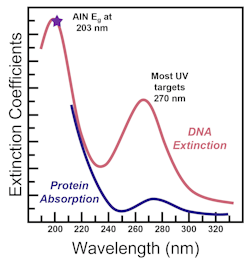
Many people are familiar with the Nobel Prize–winning discovery of using gallium nitride (GaN) — a semiconductor material with a wide bandgap of 3.4 eV — to create high-energy blue LED light. AlN’s larger bandgap results in the material’s emission of deep ultraviolet (UV-C) light with a 203-nm wavelength, which has nearly twice the energy as the 365-nm wavelength UV light from GaN.
Several companies are experimenting with and deploying UV-C light, which has wavelengths between 200 and 280 nm, for disinfection applications in healthcare or high-traffic environments, as examples. Conventional germicidal products, such as low-pressure mercury lamps that emit UV-C light with a 254-nm wavelength, can be hazardous to human skin and eyes and must be installed in locations hidden from view, such as inside mechanical ductwork. Because far UV-C light has a shorter wavelength, between 200 and 230 nm, some studies have demonstrated that it is unable to penetrate live skin cells and potentially eye cells.
Other possible optical applications for AlN LEDs and lasers could include communications, lithography, and laser-cutting, study co-author and Georgia Tech doctoral student Chris Matthews told LEDs.
The ability of the AlN semiconductor material to tolerate voltages at high levels could also help utility grids control the amount and destination of power transmitted, particularly as existing systems are being integrated with microgrid and renewable energy technologies. Both “will likely require fairly complex switched-mode power circuitry operating at very high power,” Matthews said. “In general, semiconductors with larger bandgaps can handle more power than those with lower bandgaps, and this is true for AlN as well. At 6.1 eV, AlN … should be able to handle the most power of any semiconductor material. In combination with some other properties of AlN, this means that semiconducting AlN could be used to enable smaller, higher-power transistors that are more efficient with reductions in both thermal and electrical losses.”
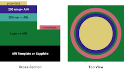
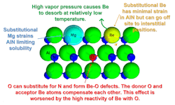
To achieve the significant conductivity improvements in p- and n-type AlN, the researchers used innovative methods to create the material. Semiconductors begin as pure elements, such as silicon, that scientists then dope with specific impurities to form crystals with targeted electrical, thermal, structural, and optical properties. Here, Doolittle and his team doped AlN with beryllium, long predicted as the best p-type dopant for AlN and GaN, according to their September 2021 paper in Advanced Materials. Furthermore, they deployed metal modulated epitaxy, a crystal growing technique, at a substantially lower temperature than typical to create the AlN crystals of the semiconductor film, which Matthews said allowed them “to avoid a number of detrimental effects like the incorporation of undesired contaminant elements and defects in the atomic structure of the AlN.”
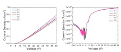
The result is a “PN AlN diode with a nearly ideal turn-on voltage of ~6 V for a 6.1 eV band gap semiconductor,” Doolittle and his team write in their May 2022 paper published in Journal of Applied Physics.
Though the potential for AlN as a semiconductor material is promising, the research is still in its early stages. Doolittle and his team are now in prototyping and optimization phases, tackling the next of many challenges, including finding a suitable contact for the UWBG semiconductor that can transport current to electrical devices. “All known metals are poorly suited to contact AlN, so metal alloys and exotic contacts will be needed,” Doolittle said in the Georgia Tech article, adding, “We have ideas as to how to push this forward and view most of these issues as engineering challenges requiring only time and resources, not fundamental science limitations.”
WANDA LAU is editorial director of LEDs Magazine and Smart Buildings Technology. She previously served as executive editor of Architect magazine and worked for a decade in the architecture, engineering, and construction industry.
For up-to-the-minute LED and SSL updates, follow us on Twitter. You’ll find curated content and commentary, as well as information on industry events, webcasts, and surveys on our LinkedIn page and our Facebook page.
