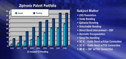
Date Announced: 30 Jan 2009 MORRISVILLE, N.C., January 30, 2009 - As the semiconductor industry explores the most effective way to implement true 3D integration of advanced semiconductors, Ziptronix is developing strategies for licensing its patented ZiBond(TM) and Direct Bond Interconnect (DBI®) technologies across the semiconductor supply chain. By licensing the Ziptronix technology, semiconductor manufacturers can quickly achieve high throughput, wafer-to-wafer or chip-to-wafer low temperature oxide bonding at the lowest cost of operation for 3D IC integration.Ziptronix, Inc., based in Research Triangle Park, NC, is a leader in IP for innovative 3D integration technology for advanced CMOS ICs, with established patent protection for its ZiBond(TM) low temperature covalent bonding (US Patent 7,387,944) and DBI® direct bond interconnect (US Patent 6,962,835) technologies.According to Ziptronix CEO Dan Donabedian, the company is uniquely positioned to deliver the low temperature IC bonding process that the semiconductor industry needs to make true 3D IC integration a practical reality. "We're currently engaged in substantive licensing discussions with customers in multiple market segments at all levels in the semiconductor supply chain, and we anticipate that several license agreements will be reached in the coming months."Donabedian explained that the Ziptronix process IP delivers important competitive advantages, and hence, increased value, at each link in the current supply chain. "Our patented bonding and interconnect technologies can be implemented at all levels of the semiconductor supply chain with little additional capital expenditure for new process equipment. In most cases, the Ziptronix technologies can be employed with slight modifications of existing tools.""The OEM/IDM customers and fabless semiconductor manufacturers can now begin to develop device designs that use true 3D integration to achieve more functionality through building multilayer chips, instead of relying on traditional 2D device scaling," he continued. "In turn, semiconductor foundries will now be able to provide their customers a high volume, high throughput wafer-to-wafer bonding process without compromising yields. And the OSATs vendors will have a repeatable, reliable method of wafer-to-wafer and die-to-wafer bonding for constructing specialized electronic modules using silicon wafers as their substrate material."In addition, Donabedian anticipated that both EDA vendors and semiconductor processing tool manufacturers would license the Ziptronix technology to enable their products to implement 3D integration as it is being adopted by the IDMs, chip designers and foundries.The company is operating from a strong base of intellectual property relating to 3D IC integration, particularly in bonding technology. "Ziptronix has developed a significant worldwide patents covering the basic concepts of low temperature oxide bonding," Donabedian continued. "Because of the depth and breadth of our patent portfolio, we believe that virtually any use of low temperature oxide bonding processes is likely to be covered by one or more of our patents."For more information about licensing Ziptronix technology, contact Chris Sanders at [email protected], call 919-459-2444 or visit www.ziptronix.com.About ZiptronixZiptronix is a pioneer in the development of low temperature oxide bonding technology for advanced semiconductor applications. Founded in October 2000, Ziptronix was spun out from North Carolina's RTI International for the purpose of commercializing their revolutionary wafer and die bonding (ZiBond(TM)) and interconnect (DBI®) technologies. The company has an extensive worldwide patent portfolio covering the fundamental concepts behind economical low temperature oxide bonding.Ziptronix technology provides the lowest cost solution for low temperature wafer-to-wafer and die-to-wafer bonding, delivering significant advantages in size reduction, lower production costs, lower power consumption and increased system performance. Ziptronix licenses its technology to customers across the entire semiconductor manufacturing supply chain - OEMs/IDMs, foundries, semiconductor equipment manufacturers and OSATs - to enable them to quickly implement reliable, economical 3D IC integration using standard processing equipment.Ziptronix Technology AdvantagesLowest cost bonding technology: According to a recent study by Yolé Development, an independent semiconductor research analyst firm, the Ziptronix DBI® process was the lowest cost bonding technique when compared to Cu-CuTC (copper-to-copper thermal compression) and adhesive technology. In their revised study results, Yolé concluded that for a typical fab running 500,000 300mm wafers per year using 1 x 20µ vias, the bonding costs per wafer level (including CMP) were: $57 for Cu-Cu; $22 for adhesive; and just $12 for the Ziptronix DBI® technology.Low temperature bonding: A key feature in the Ziptronix technology is the ability to use nickel as a DBI® metal that reliably interconnects to copper, tungsten or aluminum TSVs, while providing for adequate planarity of the oxide/metal interface to achieve a strong, reliable bond. This process supports both backside and frontside interconnects, and resolves the fundamental problem of non-planar surface depression (dishing), that typically occurs with copper. By chemically modifying the surface oxide with patented ZiBond(TM) technology, Ziptronix enables the formation of a strong, reliable oxide bond at a much lower temperature.No compression needed: Another key element in achieving the lower cost bonding is the elimination of the need for compression of the bonded wafers during the interconnect phase. The bonded wafers can be batch-processed at <300°C without compression to complete both the electrical connection at the Ni-to-Ni interface, as well as form a reliable metallic bond. Because the bonding process can be achieved using standard pick-and-place tools, there is minimal capital expenditure required to implement the Ziptronix process.Process flexibility and scaling: The Ziptronix DBI® process can be implemented for face-to-face or back-to-face configurations in wafer-to-wafer or chip-to-wafer formats to achieve high density 3D interconnects (up to 108/cm2) and is scalable to sub 1-micron pitch with improved alignment and placement tools. Ziptronix has demonstrated 3-micron and 1.5-micron pitch interconnects using existing alignment tools.Supply chain synergy: The Ziptronix 3D IC technology is available for license to OEMs/IDMs, such as manufacturers of high-performance imaging systems and sensor arrays, mobile electronics, consumer electronics and portable gaming systems; to foundries seeking to implement TSV technology and to OSATs (Outsourced Semiconductor Assembly & Test) vendors.
Contact
Beth Gaddy, BtB Marketing 919-872-8172
E-mail:[email protected]
Web Site:www.ziptronix.com


