LED lamp manufacturing costs remain high, butBARBARA STUMPPdiscusses how Molded Interconnect Device technology can deliver the 3D look and performance of a legacy bulb combined with low development and manufacturing costs.
LEDs are today unequaled among other light sources in terms of life and performance; unfortunately, the costs of solid-state lighting (SSL) systems run high. Moreover, the mechanical complexity of LED-based lamps that can mimic incandescent bulbs can add high manufacturing costs to the expense of the LEDs and thermal, optical, and driver components. Molded Interconnect Device (MID) technology can offer completely new possibilities in design freedom along with reductions in production costs for LED lamps. Indeed, the technology enables 3D structures and works with varied construction materials.
LEDs form the basis of an increasing number of lighting applications. Today, LEDs provide backlighting for liquid-crystal displays, enable a car’s brand-specific lighting design, and illuminate the 49,000-m² outfield of the Innsbruck, Austria airport without causing significant light pollution. The main advantages of LEDs are their long-term stability, the low power requirements, the low profile that enables lighting products with minimum construction depth, and a possible lifetime of some 25,000 or more hours. In order for residential consumers to partake in the power savings from LEDs, however, lower-priced products are a requisite. A new LED bulb costs up to $20 — about five times the price of a halogen lamp. Many customers will disregard the long lifetime and the lower energy consumption by nearly 80% because of the enormous price tag.
These high piece costs result in part from the structure of the LED component. It is flat and radiates to one side only. Developers turn to optics, reflectors, or the placement of LEDs in diffuser domes to achieve 300° light emission. After all, the customer wants LED lamps that look like traditional bulbs. Modern LED lamps also have a lot of additional components that can drive costs up: AC/DC conversion, light management/controls, and/or color-tunable RGB capability. A new approach to 3D design and production holds the promise of reducing lamp manufacturing costs and thereby offering headroom for the costly components used in a lamp.
Better beam patterns
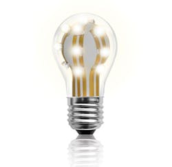
One good solution for the lamp structure and manufacturing issues is the MID process. MID enables the integration of electronic and mechanical components on a compact plastic substrate. The technique offers the freedom of placing components on a 3D structure with the location of the LEDs optimized to produce an ideal omnidirectional beam pattern. Moreover, the lamp could closely mimic the iconic shape of the incandescent lamp (Fig. 1).
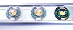
MID has already been proven technically effective in volume production of mobile phone antennas integrated in the plastic phone housing. Conductive tracks and electronic components are placed directly on a three-dimensional plastic body. The technology has also been used in an SSL product. For example, the Homelights Clip n’ Slide LED-based linear track system uses MID technology to create the body of the LED light engines that are powered through molded interconnects that make contact with the power rail (Fig. 2).
Laser Direct Structuring (LDS) technology is perhaps the most broadly used of the various MID processes and was the technology behind the Clip n’ Slide product. The basic LDS material is a thermoplastic that is doped with a laser-activated additive. A laser beam hitting the substrate uncovers the additive and forms a roughened track. The LDS additive works as a seed for the subsequent metallization in an electroless plating bath.
At Productronica 2013, LPKF demonstrated a quick prototyping process to offer a complete chain from the development of new products through volume production. So the MID process has the potential to produce future LED lamps with their numerous needed components cost-efficiently and with nearly unlimited freedom in the design of the lamps.
Electrical and thermal conduction
Ultimately in LED lamps, the LDS technology must support both the electrical and thermal needs of a product design. In general, the circuit paths are made of copper with a thickness of up to 10 µm, followed by a finish of nickel and gold. A typical LDS process enables 200-µm resolution — 100 µm in the accuracy of the interconnect path side to side and 100 µm along the length of path — for 3D structures. With an optional fine-pitch laser unit, applications with 75-µm×75-µm (line/distance) resolution are already running.
Still, LEDs require cooling, getting hot at the semiconductor junction despite their efficient conversion of electricity. “LEDs can withstand a junction temperature of 125° to 135°C continuously, and 185°C max while still delivering long lifetime,” said Rudi Hechfellner, former director of applications at Philips Lumileds and now holding a similar position at driver-IC company Maxim. “Hence, thermal management is definitely necessary, while their performance depends on the shape of the luminous element.”
For LEDs arranged linearly, aluminum rails are sufficient for cooling, according to Hechfellner — much as implemented in the Clip n’ Slide product. But 3D LED lamps need a more robust heat sink. “One needs a heat sink, which also offers the required mechanical stability and meets country-specific certifications,” added Hechfellner.
Conductive tracks on metallic bodies
One way to add the thermal element to a lamp design is a move from a plastic to a metal body. In order to simultaneously use spatial metallic lamp bodies as bearers of the components as well as heat sinks, LPKF developed two LDS-compatible powder coatings that can serve as a dielectric layer. Powder coating is already proven in mass production. The LDS PowderCoating is doped with the LDS additive and can be applied in an electrostatic process. The powder coating acts as an electrical insulator between the metallic body and conductive tracks on the surface. The coated component can be machined by the LDS process and adds electronic features to the part.
The two different powder coatings consist of the thermoset materials polyurethane and polyester. During coating, the electrically charged powder electrostatically adsorbs to a grounded workpiece; unused powder can be recovered. During curing, the coating polymerizes at 170° to 200°C, without any softening occurring throughout the course of reheating.
The LDS PowderCoating PES 200 is white, silk matte, and thermally stable. The breakdown voltage of 8.44 to 6.27 kV depends on the thickness of the coating, which ranges from approximately 80 µm.
The LPKF LDS PowderCoating PU 100 is glossy white and thermally stable with a breakdown voltage of 7.43 to 4.29 kV at layer thicknesses of 60 µm. Both powder coatings are chemically stable and UV resistant. The PES 200 provides high puncture resistance at sharp edges, while the PU 100 requires the edges to have a minimum radius of 2 mm. In terms of temperature stability the PE 200 withstands 240°C and the PU 100 withstands 270°C, both for five seconds.
Important advantages of LDS PowderCoating include the coating’s particular compatibility with electrically conducting base bodies, as well as the reflow process in which the electronic components can be soldered directly onto the base body at temperatures between 240° and 270°C. The process will also work with base bodies consisting of other materials like plastics or glass, provided that the electrical surface conductivity and the adhesion are sufficient.
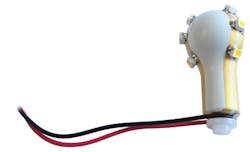
High-tech materials specialist MID-Tronic has constructed a first prototype of an LED lamp using the powder coating (Fig. 3). “A massive aluminum body acts as a heat sink, which was coated with a white LDS PowderCoating,” said Karl Görmiller, CEO at MID-Tronic. The powder coating was applied on an aluminum body and cured. Then, the conductor paths are structured by the laser and finally are metallized. This demonstrator works faultlessly, while being a bit too heavy. “First off, we wanted a functioning part,” said Görmiller. “In the future I envision a hollow aluminum body instead of a massive body, manufactured by die casting.”
Thermal management and plastic parts
Even with plastic bodies, methods are available to ensure the dissipation of heat. The production of the base body must be affordable and injection molding will be the method of choice. Because most of the heat is passing through the substrate, it is necessary to develop thermally-conductive LDS-compatible plastics to quickly transfer the heat away from the LED.
To produce suitable basic lamp bodies that act as heat sinks as well as a circuit board by injection molding, one needs special plastics that are both heat conducting and can be activated by laser. “Heat conduction in polymers can be realized by fillers,” said Christoph Heinle, director of research and development at RF Plast. But there is a potential problem. “Too much filler can make the polymer brittle,” added Heinle.
To enable lamps with plastic bodies, it is necessary to find the right mix of thermally-conductive fillers and the LDS additive for any application. “Fillers in injection-molded parts do not have the same orientation everywhere,” said Heinle. “This orientation is determined by the desired placement of the component. We are able to design suitable parts of which the heat conduction is at its maximum at the desired LED mounting place.” Heinle also said that design work optimizes the thermal effect and that material price is not a problem.
Another solution is to build thicker copper layers on plastic components. In order to achieve higher layer thicknesses of the conductor tracks (from 35 to 70 µm), one can boost them galvanically after the initial electroless metallization. “Being able to place LEDs directly on the heat sink will be a big advantage. With thermally-conductive plastic, the LDS process makes a circuit board and a thermal interface material redundant,” said Stephan Krause, strategic product manager for LDS at LPKF. “Also, the galvanic reinforcement helps to keep the LED cool.”
Pick and place on 3D-bodies
Of course, creating the electrical and thermal elements on a plastic or aluminum body is only part of the challenge in delivering a manufacturable lamp design. The concept must also enable simple installation and soldering of LEDs and other components.
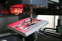
In the past, any component had to be placed manually on a basic 3D part, but this situation has changed. The Essemtec 3D placer called Hydra, for example, has been available for some time as a device for fitting a 3D-body with electronic components (Fig. 4). The system can place up to 2500 components per hour in 3D mode.
Still, there had been a problem in that gravity affects the dispensing and placing of a component on a non-horizontal surface. With the latest Hydra system, an integrated robot works inside the machine. The robot positions a substrate holder horizontally to the conventional pick-and-place arm. Glue can be applied to keep the components in place until the soldering operation is complete even when the body is positioned upside down relative to the component.
Hydra does require the developer to carefully consider design requirements. The unit can process substrates with a maximum size of 300×300×50 mm and weights of up to 2 kg with a placement accuracy of less than 60 µm. All this enables Hydra to perform in a system manufacturing application that is very close to large-scale production.
Altogether, LDS technology offers very great potential for LED lighting as the method is efficient, cost-effective, and proven for series production. With this method almost unlimited surface geometries for LED lamps are available because LDS works with free-form substrates.
Using thermally-conductive plastics instead of aluminum will further enhance productivity while allowing for quick design changes to help save money for developers bringing a new lamp to market. The LDS process allows additional electronic components and functions to be integrated without additional steps. In the future, this flexibility will make LED lamps lighter, smaller, and considerably less expensive, and enable designers to create new luminous elements.
BARBARA STUMPP is a freelance technology journalist focused on the fields of laser technologies, photonics, and industrial automation technology.


