JOHN CAFFERKEY examines the most effective packaging options for thermal mitigation in high-power LEDs, including a detailed look at the most common LED architecture and package types.
LEDs are getting brighter. To meet the demands of the general lighting market, LEDs must match the lumen output of traditional incandescent and halogen bulbs - often within the same form factor - and this mandate presents a thermal challenge, among others. The average high-brightness (HB) LED only converts around 45% of the energy put in to visible photons. The rest comes out as heat. This heat needs removing from the LED as quickly as possible to prevent the LED from overheating with potentially catastrophic failure occurring. The rise of power input in such HB LEDs exacerbates the problem by pushing far more power into the LEDs and, in turn, generating far more heat.
Interested in more articles & announcements on LED thermal management & materials?
This scenario is the thermal management challenge that is faced by LED manufacturers, and there have been a number of different approaches to overcoming it. All of these start with the LED packaging. Packaging serves a number of functions: It provides physical protection to the LED die and the method to fix the LED onto the luminaire. But it also means the LED die is then in a sealed enclosure, which largely prevents heat loss by convection and radiation. The only way to get the heat out of LEDs is by conduction from the back of the package.
This reality has led to the use of thermally conductive substrates to help minimize the thermal path between the LED and the heat sink. While it would be a simple option to use something like a slab of copper for the job because copper is an incredibly thermally conductive material, there is a catch. The thermal substrate needs to be electrically insulating since it also needs to carry the copper tracks that transport electricity to the LED. Without this dielectric, the LED would be shorted. So what the industry needs is a material that is thermally conductive yet acts as a dielectric.
LED manufacturers are constantly pushing to develop solutions to reduce cost, either by removing processes or using more cost-effective materials. The ultimate prize is to bring the overall cost of LED bulbs down to a level more palatable for a public used to paying very low prices for incandescent bulbs.
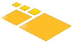
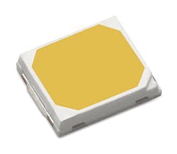
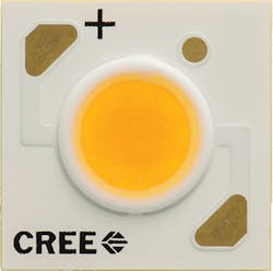
FIG. 1. Packaged LEDs come in a variety of package types including the chip-scale package (CSP) devices pictured from Samsung (top left), the mid-power LED from Lumileds (top right), and the chip-on-board (COB) LED from Cree (bottom).
Packaging options
There are broadly two approaches to HB LED packaging. Manufacturers can either package a single large LED die, or cluster of die (e.g., one red, one green, and one blue), into a device that can be assembled using surface-mount technology (SMT). Or manufacturers package a number of die directly onto what is essentially a printed-circuit board (PCB) - the chip-on-board (COB) approach. Fig. 1 includes samples of different package types from manufacturers Cree, Lumileds, and Samsung.
On the face of it, COB LEDs are a no-brainer. By mounting the bare LED die directly onto a PCB, rather than packaging the die prior to surface mounting them onto a PCB downstream, a whole process step is removed. This clearly makes COB devices a more cost-effective option.
The downside to COB LEDs is that they tend to be wide-angle emitters. These are used in luminaires such as high-bay and street lights. But where a directional light beam is required - for instance, in automotive headlights or ceiling downlights - surface-mountable HB LEDs rule.
HB LEDs and the benefits of ceramics
A key requirement for directional HB LED packaging is that both sides of the packaging substrate need to be "circuitized," with copper tracks through the substrate providing connection between the two sets of circuits. This need is critical as the packaging substrate will be mounted onto a module or luminaire circuit that needs to provide the power to the LED die. Through-holes filled with conducting copper are required but these through-holes need to be isolated from the rest of the circuit. This fact discounts materials that cannot easily have electrically isolated through-holes such as metal-core PCBs (MCPCBs).
Up until now, the only mass-market material that could meet this requirement was electronics-grade ceramic. Ceramic is ideal as it is a natural dielectric - a through-hole drilled into the substrate will be electrically isolated from the rest of the material - and certain types of ceramic are acceptably good thermal conductors.
There is another reason why ceramics are such a good choice: They are able to go through very high resolution direct-plated copper (DPC) circuitization processes. DPC is an additive process where the copper tracks are sputtered onto the ceramic to build up the circuit, as opposed to using a reductive process where the copper is removed from between the tracks using chemicals. This process builds copper up extremely accurately, to precision measured in microns, providing the fine detail required for HB LEDs.
This is where the low-cost MCPCB option again falls flat. To make the dielectric layer for an MCPCB, epoxy is added to glue the copper circuit to the surface of the metal core. It's this epoxy layer, usually mixed with grains of ceramic to improve the thermal performance, that acts as the dielectric. This can only go through a reductive process, which simply doesn't offer a high enough resolution. Again, ceramics are the only option.
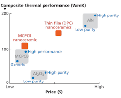
FIG. 2. Thermal material options vary in terms of thermal conductivity, ease of manufacturing, and cost.
There are two key types of ceramic used in LED packaging: Al2O3 (aluminum oxide - alumina) and AlN (aluminum nitride). Al2O3 has a poor thermal performance (20-30W/mK) but is low cost. AlN is the polar opposite. It has exceptional thermal performance (170-200W/mK), but this performance comes at high price. AlN can be up to eight times more expensive when compared to Al2O3. This presents HB LED manufacturers with a conundrum: Consciously throttle back the performance of their designs and use low-cost Al2O3 or accept the hefty price penalty that comes with AlN. Neither option is ideal. Fig. 2 summarizes the options.
Nanoceramic
However, a third option has been developed: Nanoceramic materials bring the best of aluminum and ceramic to the market. Nanoceramic is manufactured using a patented high-voltage electrochemical-oxidation (ECO) process that converts the surface of aluminum into an aluminum oxide (Al2O3). This layer is incredibly thin, measuring 10-30 μm, which is enough to act as a dielectric but its significance is that the composite thermal performance of the material is very high at 152W/mK.
Nanoceramic also overcomes the two issues that prevent standard MCPCBs from being used. Uniquely, it can be used to create isolated through-holes in aluminum PCBs. The aluminum is drilled before going through the ECO process so all surfaces - including the through-hole surfaces - are coated with a dielectric layer of nanoceramic. This creates a finished material with thermally efficient, yet electrically isolating, through-holes that can be filled with copper to build interconnects.
As the surface is Al2O3, the PCB can go through standard DPC process lines, reacting to sputtering in exactly the same way as standard Al2O3. This characteristic enables LED manufacturers to build the high-resolution circuits required for HB LEDs.
What this offers is a much-needed "middle way," providing for thermal and cost profiles that sit between the extremes of Al2O3 and AlN. Nanoceramics open up a whole new class of material suitable for all but the most challenging HB LED applications.
Matching the material and project
So what are the use cases for ceramics and nanoceramics? Here we take a broad look at HB LED scenarios where different substrates would suit. All of these classify as high-brightness applications; however, the HB LED definition is broad.
Single large-die packaged HB LED (1W). As LED manufacturers continue to drive up LED power, 1W packaged LEDs are now arguably in the mid-power camp (Fig. 3). The key factor when determining what substrate to use here will be based around power density. Where the package size is larger, the power density will drop since the amount of heat that will need removing is fixed. This would make Al2O3 a suitable substrate to use to keep the cost down. However, when the package size becomes smaller, the heat density increases substantially. Historically, this would have led to an expensive upgrade to AlN. Now nanoceramic can offer a cost-effective alternative.
Single large-die packaged HB LED (3W). Now we get into heavyweight packaged LEDs. These powerful LEDs tend to have small package sizes so they produce a lot of heat. AlN used to be the only option. Now nanoceramics can be used in all but the most extreme cases.
Multiple large die (10W). Here manufacturers place a number of HB LED die into one package to produce an incredibly powerful device. These can easily push up to 10W. Depending on the footprint, you'll be in AlN or copper pedestal territory with these devices.
FIG. 3. The discrete single-die high-brightness (HB) LED has been the industry workhorse and power levels are increasing constantly, thereby also extending the thermal challenge. The example depicted is a flip-chip device. The orange layer depicts where a dielectric material with good thermal conductivity is required.
Multiple SMT/CSP devices (>10W). Very similar to the preceding example, a light engine might use many mid-power SMT or chip-scale package (CSP) devices on a PCB (Fig. 4). If the LED spacing is sufficiently broad, it might even be possible to use standard FR4 PCB material as the substrate. But keeping LEDs cool improves life, hue, and light output. As the power density climbs, there is good reason to use an MCPCB in this application and one with a nanoceramic dielectric is the best available in this class of product.
FIG. 4. Multiple surface-mount technology (SMT) or CSP LEDs can be attached in an array to a metal-core printed-circuit board (MCPCB), and the need for thermal mitigation may be lessened with good component spacing.
Small COB array (10W). With COB devices (Fig. 5), small is definitely not cheaper! The smaller the device, the more densely packed the LED die will be on the PCB. Where you have small, superbright COB devices, the heat density is magnified. Here all available materials are on the table: Al2O3, nanoceramics, and AlN are all options depending on power density and price point for the product.
FIG. 5. An encapsulated COB LED with wire bonds can have varying thermal requirements based on the size of the array and spacing of components.
Medium COB array (10W). Now we move into larger COB devices and the power density decreases substantially. This completely changes the dynamic of the thermal challenge. With larger devices having more spaced-out die, there's also no requirement for DPC processing. MCPCB is the only way to go.
Conclusions
Thermal management of HB LEDs is absolutely not a case of "one size fits all." Each design needs to be assessed and materials selected to match the requirements. The information here gives an idea of some of the options, but at the end of the day it's always going to be a case of form, fit, and function.
The more traditional thermal substrates - MCPCB, Al2O3, and AlN - all have use cases where their particular specifications meet the requirements perfectly. However, up until now there has been a huge gap between Al2O3 and AlN where any requirement over approximately 30W/mK meant moving straight up to AlN with the huge price increase that involved. Nanoceramic changes this scenario, and offers a material that will bridge the gap between 30W/mK and 170W/mK. It's the third way - a lower-cost option to AlN for all those projects that have just gotten a little too hot for Al2O3.
JOHN CAFFERKEY is marketing manager at Cambridge Nanotherm ([email protected]; camnano.com).


