GILES HUMPSTON describes advanced materials and test equipment designed to manage and analyze the waste heat generated by LEDs, thereby improving performance across a variety of lighting applications.
When you work with LEDs day in, day out, it's all too easy to forget that LEDs and their close cousin, the solid-state laser, are actually quite wondrous. Think about it: You can connect these tiny devices up to a battery and they produce light, and not just one type of light. The wavelengths available span the far ultraviolet (UV) to the deep infrared (IR), and of course the visible range for humans. Moreover, the sources are available in a bewildering variety of sizes and power ratings. The areas of application for LEDs are expanding daily. LED TV remote controls have become LED TVs; LED torches have morphed into LED car headlights and now floodlights for sports stadiums; and new industrial products used in polymer curing, water purification, and horticulture are making tremendous advances. These myriad applications, however, face a common obstacle for reliable operation - good thermal management - and we will lay the knowledge foundation here to enable solid-state lighting (SSL) product developers to properly cool their system designs.
Interested in articles & announcements on LED thermal management?
Possibly the most notable application of LEDs today is in general lighting. As we all know, LED lights are able to produce a better quality of light more efficiently than any other source currently available. Indeed, this is one of the underlying reasons why the sale of traditional, inefficient tungsten bulbs is being progressively banned in many western countries. Factor in easy controllability and the ability to produce light sources in new and exciting form factors and it's easy to see why, according to Strategies Unlimited, the market for packaged LEDs is projected to hit $22.1 billion by 2019.
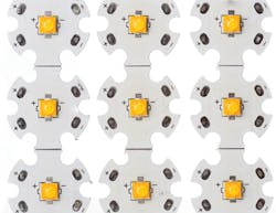
FIG. 1. HB LED packaged die can be soldered to an MCPCB "star board." The board may appear oversized for the device but is necessary to spread the heat before it meets the relatively uncontrolled interface resistance between the board and the heat sink. By spreading the heat over a larger area, a low thermal impedance path between the LED and heat sink can be achieved even if the interface resistance is quite high.
LEDs hot and hotter
A modern, good-quality, high-brightness LED (HB LED) has an efficiency of around 45%. While this might not seem particularly impressive, when you compare it to a tungsten bulb, which has an efficiency below 5%, you can see that LEDs show a huge improvement. Another way of expressing efficiency is in efficacy or lumens per watt (lm/W). HB LEDs in volume production easily achieve 150 lm/W, and the industry has a roadmap to reach 200 lm/W by 2020. This may well be achieved as research and development devices exist that exceed 300 lm/W.
The problem with LEDs is the electrical energy that is not converted to photons is converted to heat. Put simply, in operation LEDs get hot. Heat and LEDs are not good bedfellows. Heat reduces the efficiency of LEDs, so less light is produced. This effect escalates, leading to catastrophic failure. Some heat is tolerable, but operation of the semiconductor much above 100°C noticeably reduces the quality of the light produced and triggers a variety of wear-out mechanisms that considerably shorten the life of an LED bulb.
Because the operating temperature of LEDs needs to be relatively close to ambient, the only effective means for removing heat is by conduction. The upshot of this is that HB LEDs need to be attached to a type of circuit board that is specially engineered to transport heat by conduction through to a heat sink. The various circuit board types are known by names including insulated metal substrates (IMS), metal core or clad printed-circuit boards (MCPCBs), and metal-in-board printed circuit boards (MIB PCBs).
Measures of thermal performance
A prospective manufacturer of LED lighting products needs to select a thermally conductive circuit board that is suitable for the chosen brand of HB LEDs. This should be a simple matter of looking through datasheets from various MCPCB manufacturers and selecting one that delivers adequate thermal performance for the price. But to do so requires an understanding of the available measures of thermal performance. Without this, it is easy to be misled.
For example, consider thermal conductivity. A good conductor of heat, like copper, has a high thermal conductivity of 394 W/mk (watts per meter kelvin), whereas a poor conductor of heat, like alumina (aluminum oxide), has a low thermal conductivity of 25 W/mK. On this measure it would appear that a circuit board made with a copper core will keep LEDs much cooler than one with an alumina core. This conclusion is not necessarily correct. Thermal conductivity is normalized to a dimension, so unless the area and thickness of the core are specified, comparison is impossible. To put it another way, an alumina board that is 1.5 mm thick will outperform a copper board of the same area that is 25 mm thick.
Thermal resistance is a far more useful comparative measure of thermal performance for circuit boards that remove heat from LEDs by conduction. Thermal resistance is thickness divided by thermal conductivity. Now we can see that the copper board in the example above has a thermal resistance of 0.063°C∙cm2/W and the alumina board trumps it at 0.060°C∙cm2/W.
Thermal resistance
The great thing about thermal resistance is that it can be used to analyze the layers in a complex structure like a thermally conductive circuit board for an HB LED (Fig. 1). Starting from the top down, the first layer will be copper tracking in either one-, two-, or occasionally three-ounce weight (35-, 70-, or 105-μm thickness). Mostly, HB LEDs will be soldered to the copper tracking. Beneath the copper will be a dielectric. This will typically be a thermally conductive epoxy around 75 μm thick, but more advanced solutions based on nanomaterials are available for designs where particularly low thermal resistance is required.
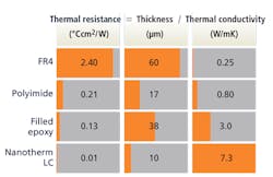
Fig. 2 compares the thermal resistance characteristics of some popular dielectric materials commonly used in MCPCBs. Thermal conductivity does not provide the information to rank materials. The minimum thickness depends on multiple factors including manufacturability, reliability, and the withstand potential of the dielectric.
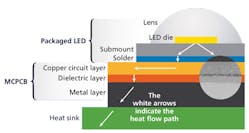
The dielectric will be supported by a metal core. Despite its thermal advantages, copper is mostly shunned in favor of aluminum on the grounds of cost, weight, and expansion match to the heat sink, which in all probability will be aluminum. A thermal interface material (TIM) is often inserted between the heat sink and the MCPCB because the MCPCB and heat sink are unlikely to be totally flat. A TIM is a physically compliant material that deforms to ensure there are no gaps in the joint because even a thin layer of air has very, very high thermal resistance as the thermal conductivity is so low (0.024 W/mK). Fig. 3 depicts the typical material stack in an LED assembly.
Calculating the total thermal resistance between the HB LED and the heat sink is quite straightforward. It merely entails adding the thermal resistances of the individual layers. While this is a major advance on using thermal conductivity as a measure for comparison, to have any hope of predicting the operating temperature of an HB LED and especially where the thermal path is more complex, we need a different thermal unit - thermal impedance.
Thermal impedance
Thermal impedance is thermal resistance of a specified component. This means the entire thermal path can be modeled by summing all of the series and parallel heat paths. For example, an MCPCB might have a datasheet thermal resistance of 1.0°C∙cm2/W. Note the units of area. This means if the MCPCB measures 4 cm2, the thermal impedance will be 0.25°C/W. If the MCPCB is bolted to a heat sink so the bolts provide an additional thermal path in parallel to the MCPCB, they will contribute to cooling of the LED. Say there are three bolts, each having a thermal impedance of 5°C/W; then the combined thermal impedance of the board and bolts becomes 0.21°C/W, derived from Rtotal = 1 / (1/r1 + 1/r2 + ...+ 1/rn).
FIG. 2. Four different common dielectric materials exhibit vastly different thermal characteristics.
Heat sinks are sold as components having a thermal impedance rating, for example, 0.7°C/W. This means we now have sufficient information to calculate the operating temperature of an LED. Take a 100W LED by way of example; due to the inefficiency, there is 55W of heat to dissipate. The thermal path from the LED to air, through the MCPCB, bolts, and heat sink is 0.21 + 0.7 = 0.91°C/W. At 55W the thermal step across these components will be 50°C (0.91 × 50 = 50). So if the ambient is at 25°C, the HB LED will be running at 75°C - very approximately!
Approximations, models, and interface resistance
Heat always flows from hot to cold. HB LEDs are physically small devices, typically around 1 mm2, whereas heat sinks and MCPCBs are much larger. This means the heat not only flows vertically through the structure, but some travels laterally out toward the perimeter. From a thermal perspective, it might seem that having a large, thick copper pad under an LED is a good idea. Yet again the picture is not quite as simple as that. For LED devices with extreme cooling requirements, the best-in-class MCPCBs have an aggregate equivalent thermal conductivity approaching 100 W/mK (data sheet value with dimensions not specified).
FIG. 3. The illustration details the schematic thermal heat path from an LED die to a heat sink. The LED die approximates to a point source. Layers of high thermal conductivity over a layer of high thermal resistance spread heat laterally. To achieve low thermal impedance from the LED to the heat sink, it is important to spread heat ahead of layers with high thermal resistance. The inset shows a commercial MCPCB highlighting the importance of achieving a very thin dielectric layer.
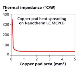
The structure comprises an aluminum plate, one surface of which is made insulating by conversion to nanograin alumina. Because nanograin alumina is a very good dielectric (>50 V/μm), only a very thin layer is required so its thermal resistance is very low. The copper tracking is glued on top. Although the glue line is exceedingly thin, the low thermal conductivity of unfilled adhesives (typically 0.2 W/mK) means there is a thermal barrier right underneath the die. With no heat spreading, the thermal resistance is atrocious. But, by increasing the dimensions of the copper pads only slightly, the heat from the LED is spread over a larger area and this substantially decreases the thermal impedance. Fig. 4 shows a sample graph of thermal impedance relative to copper pad area.
In a structure with multiple layers and parallel paths, the only way to properly predict the operating temperature of the HB LED is to construct a finite element model. While a finite element model will provide a big step forward in understanding the thermal performance of a system, the accuracy of the result will be severely hampered by two factors. They are interface resistance and the measured performance of the MCPCB.
Interfacial thermal resistance, to use its proper technical name, arises wherever two materials abut. It exists at even perfectly joined interfaces. Due to reasons of physics, a proportion of the heat attempting to flow from hot to cold gets scattered at interfaces and sent off in a less useful direction. From a model perspective, interface resistance can be included as an additional layer with an associate thermal resistance. The difficulty is in knowing what numbers to assign since real-world values are influenced by a host of variables that are difficult to control. To complicate matters further, interface resistance is not usually stable and will alter over time due to minute changes in the material properties, form, and macro proximity of the abutting surfaces.
Similarly, measurement of the thermal resistance of MCPCBs is not straightforward. They are complex, multilayered structures containing a number of internal interfaces. The common methods of measuring the thermal resistance of MCPCBs are the axial flow and laser flash techniques.
Measuring thermal properties of MCPCBs
In the axial flow method, the MCPCB is sandwiched between a hot plate and cold plate. By recording the power required to maintain a temperature difference across the sample, the thermal impedance, thermal resistance, and thermal conductivity can be derived. The laser flash diffusivity employs a laser to deliver a short pulse of heat to the front face of the sample and an IR camera observes the temperature change at the rear face as a function of time. Some clever mathematics are then used to de-embed the thermal properties.
FIG. 4. The graph details the calculated thermal resistance between an LED die (250 μm per side) soldered to a copper pad on a Nanotherm LC MCPCB (1.5-mm aluminum, 20-μm nanograin alumina) as a function of the copper pad area. The finite element model includes estimates for internal interface resistances. Heat spreading in the copper pad is essential to achieving low thermal impedance due to the thermal barrier presented by the thin adhesive joint between the copper and the nanograin alumina dielectric.
While both methods work well for homogeneous materials, when presented with a multilayered component where the constituent layers can have thermal conductivity differences of two orders of magnitude, the results never quite agree. It is generally found that when evaluating an MCPCB, the laser flash technique measures a lower thermal resistance. There is therefore no need to guess which method manufacturers prefer to populate datasheets.
The preferred method of ascertaining the thermal performance of an MCPCB used to cool HB LEDs is to measure it, using a live device. The forward voltage drop of semiconductors like LEDs is a very precise and reproducible characteristic. For gallium-nitride (GaN)-based LEDs, the diode junction has a temperature coefficient between -3 and -6 mV/°C, depending on the exact type of semiconductor. By measuring the forward voltage drop at a known temperature, it is then possible to do the contrary and derive the device temperature from the forward voltage drop under other conditions.
The HB LED is attached to an MCPCB which in turn is fixed to a temperature-controlled heat sink. The HB LED is powered up and the junction temperature determined from the measurement of the forward voltage drop of the p-n junction (under highly specific conditions). The thermal impedance to the heat sink, including real-world effects of heat spreading and interface resistances, is then obtained. Even better, by pulsing the LED and deploying some fancy instrumentation and mathematics it is possible to work out the contribution of every single component and interface to the total thermal impedance between the LED junction and the heat sink. The graphical form of the data is colloquially referred to as the "cumulative structure function." The complexity of this test method has been greatly diminished by the appearance of commercial equipment specifically engineered to the task.
Lumen output
No matter how sophisticated the thermal model or measurement system, provided the HB LED is operating at a safe temperature, what actually matters is the quantity of lumens produced. More specifically, the brightness at the wavelengths of interest. A tungsten filament bulb is actually extremely efficient (>90%) if you include all of the IR photons produced.
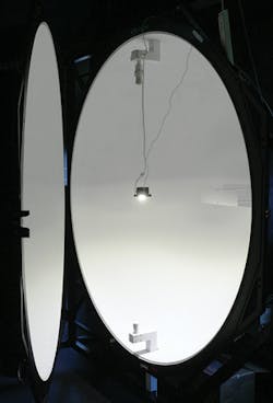
FIG. 5. A 150W LED light on a fan-assisted heat sink is suspended in an integrating sphere. This instrument permits the total light output to be measured as a function of wavelength. The photo is from the facility of The Lighting Industry Association Laboratory, a fully accredited test laboratory dedicated entirely to the testing of light sources and luminaires.
Measurement of total optical output from luminaires and LED modules is accomplished using an integrating sphere (Fig. 5). These circular chambers are coated with highly reflective paint, enabling collection of all of the light produced from the source irrespective of the direction and wavelength. Where the light from a lamp is confined to a cone or other pattern, a goniophotometer is often used instead. This is essentially a photometer that measures the angular dependence of optical quantities. In addition to the luminous intensity distribution, a modern instrument can usually also provide the luminous flux, spatial color distribution, luminance, and other optical information about the light source. Knowing the electrical input to the HB LED and specifying a wavelength span, beam angle, and hue permits quantitative determination of the electro-optic efficiency of the light source.
Conclusions
LEDs are semiconductor devices designed to generate light. But the modest efficiency means considerable quantities of waste heat are generated in the process. This heat must be removed by conduction; otherwise, the performance of the LED suffers and ultimately its life will be shortened. To meet this challenge, special circuit boards have been developed that have exceptional through-thickness thermal conductivity. Simple calculators can be used to give an approximate guide to the performance of a given thermal management solution provided care is taken to use appropriate thermal units.
Reasonably precise models of thermal performance can be constructed using a finite element approach, but accuracy can be hampered by a lack of reliable values for interfaces. Measurement of the thermal properties of multipart components like MCPCBs is complex and the values obtained can depend on the approach used. Advanced test equipment exists that is able to produce a detailed picture of all the elements that contribute to the total thermal impedance between a live LED and heat sink. Stating the electro-optic efficiency of an LED light source requires specification of multiple parameters including electrical input, die temperature, wavelength span, beam angle, and hue.
GILES HUMPSTONis applications manager at Cambridge Nanotherm (camnano.com).

