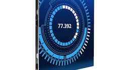
Date Announced: 27 Aug 2013 Washington D.C., USA - AZZURRO LED Technologies announced the breaking news during a talk at ICNS-10. While showing production values of less than 3 nm wavelength uniformity, the 1.0 nm result came straight from development. The record 1.0 nm result demonstrates the capability to achieve "1 bin" GaN-on-Si LED wafers with AZZURRO's technology.After questions about achieving competitive brightness and efficiency levels have been answered by various GaN-on-Si contenders, the yield question has remained open. The large mismatch of crystal lattice structure and thermal expansion coefficient cause highly bowed LED wafers after and during growth. This in turn has a very big negative impact on uniformity levels for wavelength, forward voltage and output power. AZZURRO uses its proprietary and patented strain-engineering and growth technologies to overcome these obstacles.Breakthrough uniformity from production for wavelength (<3 nm or 0.6%), forward voltage (1.3%) and output power (3.9%) for highly reduced binning were shown at the ICNS-10 in Washington D.C., USA together with excellent crystal quality values for 150 mm blue emission GaN-on-Si LED wafers (all values are standard deviation). At the same time equally impressive values for 200 mm LED wafers show AZZURRO's technological scalability. Manufacturability parameters like low bow (<20 μm) and very good thickness uniformities (1.7%) are not compromised on. Based on these achievements the technical team continues to push for the ultimate "1 bin" wafer aim and demonstrated the benchmark result for wavelength with only 1.0 nm uniformity and a min/max value of 5 nm (one wavelength bin). See graph to the right.AZZURRO's latest results from production and development clearly prove that in addition to the cost advantages from lower cost substrates and by using standard silicon fabs for LED chip processing GaN-on-Si LED wafers with the right strain-engineering technology can also help reduce binning dramatically.AZZURRO's co-founder and CMO, Alexander Loesing, who is also heading its LED Technologies business unit, commented on the results: "We are very proud of our team's record 1.0 nm achievement. With these results we show that our GaN-on-Si technology can bring the LED industry closer to the aim of making '1 bin' LED wafers."About AZZURRO SemiconductorsAZZURRO has pioneered the growth of gallium nitride on silicon substrates (GaN-on-Si). The company manufactures epitaxial wafers for LED and power semiconductor applications. The use of AZZURRO's large wafer diameter GaN-on-Si strain-engineering technology allows both industries to facilitate standard semiconductor production sites to enable massive cost savings.About AZZURRO LED TechnologiesDifferent from AZZURRO's established wafer manufacturing business this recently formed business unit has the sole purpose to enable the LED industry's migration to GaN-on-Si. All LED experts, facilities and know-how as well as IP within AZZURRO are gathered in this business unit to put all necessary resources behind the strategy to demonstrate GaN-on-Si LED in the first phase and in the second phase to license and transfer AZZURRO's technology know-how and IP to the LED industry.
Contact
Alexander Loesing, AZZURRO LED Technologies @ AZZURRO Semiconductors AG +49-351-212-99 x128
E-mail:[email protected]
Web Site:www.azzurro-semiconductors.com