This article was published in the September 2011 issue of LEDs Magazine.
View the Table of Contents and download the PDF file of the complete September 2011 issue.
+++++
As demand for high-brightness LEDs continues to accelerate, manufacturers are turning to a potent combination of yield analysis, process control, equipment monitoring and factory automation to increase output, optimize profitability and gain strategic advantage in an increasingly competitive marketplace. While each of these components brings specific benefits, when intelligently integrated, their total combined benefit is far greater than the sum of their individual contributions.
Historically, LED manufacturing has suffered from low overall yields and even lower binned yields of devices with specific characteristics. High yield variability further complicates the problem, introducing significant uncertainty over time and making it difficult to maintain a nimble yet reliable supply chain for customers. As the market matures, it is no longer economically viable to simply buy more capacity, and competitive advantage will shift increasingly to those who can improve yield and increase output through more efficient use of existing assets.
In addition to rapidly-growing demand, other trends in the industry are also increasing the pressure to improve yields. These include demand for larger LEDs in a single package; the need to reduce assembly costs and reduce losses to “street waste” (between die); as well as increases in the number of die per wafer, resulting from smaller die and larger wafers.
Yield management
Yield management provides the capability to analyze defect, metrology and test data across the entire process. Input data should be collected as widely as possible, including inspection and metrology tools, equipment sensors and event logs, manufacturing execution system (MES) scheduling and tracking data, and final test yields.
Given sufficient input, yield analysis can quickly determine where the root cause of a problem lies - incoming material, equipment malfunction, or process excursion. It allows engineers to prioritize their efforts on those problems that have the greatest effect on yield. Once a cause is identified they can drill down further to equipment-performance data, formulating procedures to prevent future process problems.
Although much of the methodology for LED yield analysis can be adapted straightforwardly from integrated-circuit manufacturing, LED manufacturing also poses a number of unique challenges. These include the ability to process data from broken or partial wafers, the precise alignment of maps among various tool sets, and the ability to simultaneously analyze thousands of wafer maps each with hundreds of thousands of die.
In the second example, engineers were challenged to find the cause of sporadic low-yielding wafer lots. The yield management system (YMS) allowed them to select over 1,000 wafer maps from low-yielding lots and stack them to look for tell-tale patterns in the defect data. The maps first had to be aligned to correct rotational errors of plus/minus several degrees that result from the “one-shot” exposure technique used for LED fabrication. Then, using algorithms specially designed to recognize wafer-scale spatial patterns, they were able to trace the problem to the bonding process (Fig. 2). The entire analysis, which would likely have taken several days to perform manually, was completed in less than two hours.
YMS can also be used to correlate yield with event-type data such as changes in recipes, equipment maintenance, SPC alarms and more. Quantitative data on the yield impact of these occurrences, which may include aggregate data from multiple sources, provides a sound basis for operational decisions, such as the optimal frequency of periodic maintenance procedures. Periodic reporting and charting focuses engineering resources on important yield-robbing issues. Automatic alarms can trigger customized reports that drill down through the data to reveal underlying causes.
Equipment monitoring
Real-time fault detection and classification (FDC) tools analyze hundreds of data points per second to monitor equipment performance. Using this data, it constructs models to predict process performance based on the monitored parameters. Engineers can use the models to detect abnormalities before they become faults. Automatic characterization of faults reduces trouble-shooting time. Accurate models also allow the optimization of maintenance schedules to provide maintenance when, and only when, it is needed, avoiding unnecessary downtime and minimizing cost of ownership.
Fig. 4 demonstrates the value of real-time FDC on a CVD tool. Without real-time monitoring, 138 wafers were misprocessed before the problem was detected and it took 3.5 days to locate and correct the fault. An FDC model was developed that detected the fault on the first misprocessed wafer, informing engineers of the exact nature of the problem to speed repairs.
Process control
By monitoring drifts in process performance from run to run, engineers reduce process variation and drive performance to optimal values. Possible applications include control of film thickness, composition, and uniformity; critical dimensions of metal lines; the accuracy of pattern overlays; and thermal uniformity during the growth of multi-quantum wells. Automation of run-to-run measurements and adjustments reduces engineering time and eliminates operator errors in the calculations. Avoiding rework and increasing the time between replacements also improves the cost efficiency of consumable parts and supplies.
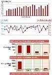
Chemical mechanical polishing (CMP) processes remove material from the wafer surface using a chemically-reactive, abrasive slurry and a polishing pad. The material removal rate changes as the pad ages. By measuring the removal rate of the process combined with feed-forward thickness information and feeding this information back to modulate down-force and polishing time for the next run, engineers were able to reduce film-thickness variability, center variations about the target value, and maintain the process entirely within control limits (Fig. 6).
Factory automation
The final piece of the puzzle is provided by the factory automation system, which coordinates the data flow between operators, equipment and factory systems. It provides communication among all systems and components in the factory, including user interfaces and credentials, engineering enquiries and reports, process control systems, data collection interfaces, process equipment, operational settings and recipes, databases, and incoming material entry. The implementation of well-designed automation layers significantly reduces the time to implement advanced analysis packages, such as fault detection and run-to-run control systems, and virtually eliminates scrap due to operator error.
Comprehensive integration among the various components – yield analysis, fault detection and classification, and run-to-run process control – is the key to maximizing returns on investment in process control. Yield analysis, including automatic defect classification and spatial pattern recognition, permits the rapid identification and prioritization of yield-reducing problems and their root causes. Fault detection and classification permits predictive modeling to detect abnormalities and trends before they impact yield. Run-to-run process control allows feedback of current process performance to adjust operating parameters, achieving better control and tighter process windows. Moreover, all of these technologies can scale inexpensively to accommodate additional process capacity.
Given that some current LED manufacturing processes have yields less than 40% and binned yields less than 20%, yields could double and binned yields could quadruple and still be at levels well below those of advanced IC manufacturing processes.
Although there may be unknown practical impediments to achieving such yields for LEDs, the mere possibility of such dramatic increases in productivity, with only modest investments in control systems and little or no investment in additional process equipment, is sufficient to stimulate intense interest among manufacturers.


