The HB-LED Standards Committee met for the first time on November 11 and initiated standards Task Forces on wafers, carriers, assembly and automation. The Committee and Task Forces are comprised of industry leaders in HB-LED devices, sapphire wafers, MOCVD wafer processing, and key equipment and materials suppliers to the LED industry.
The overall HB-LED market will grow a remarkable 68 percent this year to reach $9.1 billion, with projections of doubling in size to $18.4 billion by 2014, according to industry analysts at Strategies Unlimited. This high-growth phase is currently driven primarily by LED TVs, displays, mobile phones, and other portable devices. However, the next growth phase of HB-LEDs will result from increasing demand for solid-state lighting where significant cost reductions will be required to replace conventional lighting sources.
Industry analysts expect a 10- to 20-fold decrease in costs over the next five years to achieve rapid penetration of solid-state lighting into commercial and residential lighting applications. The SEMI HB-LED Standards Committee has been formed to help reach those aggressive cost targets.
During its inaugural meeting, the HB-LED Standards Committee agreed to form task forces in four critical areas of LED manufacturing:
- Wafers: Unlike silicon wafers used in semiconductor manufacturing, there currently are no industry standards addressing wafer geometries, surface characteristics, wafer ID, wafer orientation, and other features, resulting in costly proliferation of wafer types and styles. The objective of this Task Force will be to analyze and develop wafer standards (starting with sapphire wafers) that will reduce the proliferation of varying wafer types on the market — thereby reducing costs and enabling manufacturers to focus on true product and process innovation.
- Carriers: Wafer carrier standards will enable lower cost, higher precision, and more productive wafer handling, shipping, and processing. The Task Force is expected to develop standards for shipping carriers (used to ship the virgin wafers from the wafer supplier to the customer), automation carriers (carries the wafers through the automated tools), and process carriers (used to carry wafers into and from process tools; may be subjected to aggressive environments (chemical, liquid, thermal).
- Automation: The objective of the Automation Task Force is to analyze and develop industry standards that allow low-cost, common hardware and software interfaces, and other means to enable HB-LED factories to effectively utilize multiple equipment types from multiple vendors in a highly automated and integrated fashion.
- Assembly: Currently, wire bonding and other assembly steps are highly varied depending on the unique optical, thermal, and electrical requirements of today’s advanced lighting applications— resulting in higher costs and lower throughput. The objective of the Assembly Task Force is to examine industry standards — relating to issues like machine vision, device orientation, handling interface, and other areas — that will enable lower-cost, higher-throughput assembly while recognizing diversity of component types in a typical HB-LED manufacturing environment.


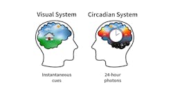
![FIG. 1. The timeline of light sources relied upon by humans has evolved from one focused on the source of illumination for visual acuity alone to one that applies advanced research to evoke or inhibit certain responses from the non-visual system. The research will deliver new information to the solid-state lighting (SSL) industry for producing metrics that enable standards and best practices development for products and lighting designs. [Image credits: All illustrations courtesy of Allison Thayer, the Lighting Research Center (LRC).] FIG. 1. The timeline of light sources relied upon by humans has evolved from one focused on the source of illumination for visual acuity alone to one that applies advanced research to evoke or inhibit certain responses from the non-visual system. The research will deliver new information to the solid-state lighting (SSL) industry for producing metrics that enable standards and best practices development for products and lighting designs. [Image credits: All illustrations courtesy of Allison Thayer, the Lighting Research Center (LRC).]](https://img.ledsmagazine.com/files/base/ebm/leds/image/2020/08/2009LED_tha_z1.5f483ea7ebf0d.png?auto=format,compress&fit=crop&q=45&h=139&height=139&w=250&width=250)