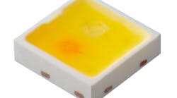
The TFFC process involves removal of the sapphire substrate and roughening of the chip's light-emitting surface to improve light output efficiency. The company says its TFFC design is optically and thermally superior to competing chip architectures.
"TFFC technology allows us to maximize the light emitting area and minimize thermal resistance, resulting in brighter and more efficient LEDs," said Frank Steranka, Executive VP of Research and Development at Philips Lumileds. "These attributes are required for applications in general lighting, automotive lighting, display, and projection to name a few."
Steranka said that white Luxeon LEDs with TFFC are capable of delivering more than 80 lm/W at 350mA. Using its TFFC technology, the company expects to introduce 100 lm/W and higher white LEDs in the coming year and will push the efficacy to 150 lumens/watt and above in the longer term.
Earlier this year, Lumileds' Advanced Labs group claimed a record 115 lm/W performance for a power LED (see Philips Lumileds reports 115 lm/W power LED at 350 mA). "We will continue to move technologies from our Advanced Labs group into R&D and Manufacturing," said Steranka. "This process provides for a continuum of performance improvements in the chip, phosphor, and packaging areas."
TTFC chip design
In Lumileds' process, the gallium nitride (GaN)-based LED chips are fabricated by depositing multiple layers of GaN-based materials onto a sapphire wafer. Electrical connection points (anodes and cathodes) are fabricated on the top surface of the GaN wafer. The wafer is flipped upside down (hence the term "flip chip"), and the anodes and cathodes are bonded using gold interconnects to a suitable submount or package.
Next, a laser is used to remove the original sapphire wafer, leaving only the thin layers of GaN-based material (hence "thin film"). Then, an etching process is used to roughen the top surface of the chip, which disrupts the wave-guiding of light within the GaN layers and leads to more light emission through the top surface – leading to improved brightness.
Some alternative approaches to the TTFC approach use a high reflectivity metal layer to bond the GaN layers to the submount. After sapphire removal, it is necessary to add a mesh-like contact layer and a wire bond to the upper surface of the structure. The patterned mesh reduces the emitting area of the chip, while the wire bonds limit the proximity of the primary optics to the chip.


