Custom LED displays for instrumentation and message panels

Oct. 15, 2004
Geoff Lidgard of PRP Optoelectronics Ltd describes the design, development and manufacture of small-scale custom LED arrays for instrumentation, message panels and imaging equipment.
LEDs are used in a wide variety of display applications ranging from large outdoor display screens with dimensions measured in metres to high-resolution arrays with emitters as small as 10 microns. Within this broad field, PRP Optoelectronics Ltd has specialised in the design, development and manufacture of smaller-scale custom LED arrays for instrumentation and message panels, mainly for avionic applications, as well as multi-element fine-geometry monolithic arrays for display and imaging equipment.

The arrays are based on two different technologies, hybrid and monolithic, depending on the application, although there is some cross-over where displays using a monolithic LED chip are packaged with controlling or matching hybrid electronic components.

Hybrid displays

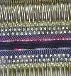
Figure 1a These are made using hybrid electronic assembly methods in which individual LED die are assembled onto the front face of a multi-layer ceramic package or PCB in the required display pattern. The electronic drive circuitry, typically consisting of custom ASICs, memory devices and FETs etc. is mounted onto the rear face of the package or PCB. The device is then completed by fitting a suitable window and/or filter to the front of the package and a cover to the rear protecting the electronics.
Figure 1b The display layout is very flexible and can range from a set of 7 x 5 characters to a full XY matrix, or even a circular pattern mimicking a moving pointer instrument. The LED die are generally 0.28mm square spaced on a 0.5mm pitch, but other sizes and custom rectangular bar shaped LED die are used on some displays, in particular for circular instrument panels.

As single LED die are used, it is possible to mix and match any of the wide range of LEDs that are now available, and so multi-colour displays with blue, green, amber or red emitters can be made. Figure 1 shows an example of an amber circular display showing the patterns on the front (LEDs) and rear (drive electronics) of the package together with the fully-illuminated display. This particular device, in addition to acting as an analog display, can also show the measured value as a rolling-digit digital display.

Figure 2 The LED dice are viewed directly and there is no epoxy encapsulation over them acting as a lens. This means that the displays, if fitted with an appropriate contrast enhancement filter, can be easily be seen in direct sunlight allowing them to be used on aircraft flight decks. It is also possible with suitable pulse-width modulation (PWM) driving techniques to dim the display down to very low levels so that they are also compatible with night vision systems. For some applications, fixed legends are needed and in this case back-lit screen-printed windows are used with the LED dice embedded in a diffusing medium. Again, with suitable optical design, these can be sunlight visible.
Figure 3 The window/filter can be either glass, plastic or a combination of both to provide the correct transmission characteristics, and is usually fixed to the package with an epoxy or silicone glue. As the LED chips are themselves relatively robust, this type of structure usually provides sufficient protection in most normal environments. However for use in extreme conditions, particularly high humidity ones, a conformal coating such as Parylene can be deposited over the chips before the window is fitted to protect the LED dice, the chip bonds and the package metallization.
Figure 4 LED displays operate over a very wide temperature range and it is usually the mechanical components such as the (plastic) filters or adhesives that limit the operating temperature range of the units. The assemblies are mechanically very robust and the LEDs have lifetimes of at least 105 hours. These characteristics make this type of display ideally suited to high reliability applications. Further examples of this type of displays are in Figures 2 to 4.

Monolithic arrays

These are multi-element emitters on a single chip with each of the emitters having a separately addressable connection (usually the anode) to allow it to be driven independently, and a common (cathode) return connection. The emission areas can vary in size from a few microns across, while the formats and spacings that can be produced depend on the need for contact metallizations to make contact to the emitting regions.

Obviously a separate connection and hence wire bond for each element is required and therefore the wire bond pad layout is usually the factor that limits the size of a chip. To overcome this limitation, XY matrix addressable arrays are currently under development.

Figure 5a These kinds of arrays can be made by a variety of techniques such as diffusion, mesa etching or implantation. As they are produced in the same way as an IC on a complete epitaxial wafer, and the area of material used for each chip is relatively small, the uniformity of emission and colour across a chip is well controlled.
Figure 5b Individual emitting areas vary from 10 microns across and linear arrays with up to 512 emitting areas on a chip are being used in commercial applications, while the development of the XY arrays with thousands of emitters is underway. Arrays can be made with the full wavelength range from blue through to red for visual applications and into the infra-red for machine applications. These types of array are used in thermal imaging displays, head-up displays and helmet-mounted sights. They are also used in reprographics, high speed printing, PCB patterning and can potentially be used for lab-on-a-chip applications.

The LED chips can be mounted into a variety of packages depending on the intended use, and this can include optical components (such as lenses etc) and/or electronic components to provide local LED drivers or output matching. The emission levels across an array are usually matched to within a few percent as processed, but this can be improved by the inclusion of either active matching using previously stored coefficients, or passively by the use of pre-determined resistor networks. Examples of various types of device and packages are shown in Figure 5.

Figure 6 A close up view of an array with a double row of emitters that has some of the elements illuminated is seen in Figure 6. This has elements measuring 30 microns across and spaced on a 42 micron pitch. The typical forward intensity obtained from this type of array, emitting at a wavelength of 650 nm, is 80 micro-W/steradian (~ 1 x 10⁷candela/m2) when driven at an element current of 10 mA.

Most applications of monolithic arrays use one or two chips per unit, but for some printing applications, wide print bars are required. In Figure 7 we can see such a unit. This particular example is 20 inches wide with emitters spaced at 600 dpi. Individual linear arrays are assembled end to end to maintain the 600 dpi spacing along the full length of the bar.
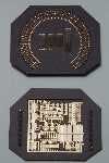
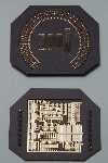
Figure 7 These examples show some of the typical formats of monolithic arrays that are used, but it is possible to produce other types of layouts, ranging from small seven-segment numerics to compound displays with characters and symbols, such as reticules and geometric overlays for optical instruments.