Download a PDF version of this article (0.9 MB)
As the LED industry evolves, demand increases for efficient, high-brightness light sources. The approach of chip manufacturers, such as Lumileds and Osram, has been to make bigger die and drive them harder, as well as improving light extraction efficiency, in order to get more light out. This works well for applications requiring tens of lumens, but not necessarily for brighter light sources.
"Companies that build LED arrays using packaged LEDs are starting with the limitations of a packaged part - it has a fixed thermal resistance, and you can only package the die as close together as the package will allow," says Joe Mazzochette, Lamina's VP of Engineering. Instead, Lamina's approach is to work with the best available bare die and package many of them very close together using a thermally efficient packaging material.
Metal laminate structure
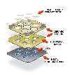
The packaging technology utilized by Lamina is Low-Temperature Co-fired Ceramic on Metal (LTCC-M), in which the metal substrate is a copper-molybdenum-copper laminate. The package benefits from a high thermal conductivity associated with copper, but at the same time has a very low thermal coefficient of expansion (TCE) that is matched to the semiconductor material of the LED die. This significantly reduces the stresses caused when the materials expand and contract during thermal cycling.
"TCE mismatches are very important - turning parts on and off stresses the die even if you can control the ambient temperature very accurately," says Mazzochette. "In simple T-packages, the die temperature can be 75°C higher than ambient." Longer term effects can also stress the material, for example in outdoor applications where the temperature ranges from -30F in the winter to 100F in the summer. Repeated stressing of epoxy joints and solder bonds within the package often results in failure, even though the LED die may still be functional.
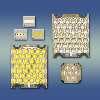
On top of the metal substrate the package has multiple ceramic layers that carry electrical traces. The LED die sit inside cavities punched into the ceramic layers. Each cavity can contain multiple RGB die, which greatly improves color mixing compared with arrays of RGB packages. Lamina's BL-3000 series RGB light engine has 39 cavities, each containing multiple red, green and blue die. Also, additional circuitry - electro-static discharge (ESD) protection, drivers, temperature compensation - can be packaged on the substrate.
Flip-chip bonding
In other structures, notably the Lumileds Luxeon package, the die is mounted on a silicon submount, due to the difficulties of bonding LED die directly to a copper heat sink. Although processes such as flip-chip bonding to silicon are well understood in the semiconductor industry, the silicon submount adds an extra layer of thermal resistance and also has to be glued to the copper heat sink.
The low TCE value of the Cu-Mo-Cu laminate reduces problems of mismatch between the substrate and the solder or gold that is generally used to fabricate the flip-chip stud bumps - temperature cycling can cause solder to stress and crack, which ruins the electrical and thermal connections in the flip-chip assembly.
The silicon sub-mount is used for ESD protection, but also as a TCE buffer between the metal core and the LED die. The sub-mount has to be larger than the die, and the expansion problems get worse as the die get larger, in contrast to Lamina's approach. "All of the things that make Lamina's technology useful become more important as the die run at higher powers and higher temperatures and as they get larger," says Anderson.
Performance and cost
The advantage of combining multiple die on a single substrate means that Lamina's packages are some 3-10x brighter per unit area that arrays made by combining individual LED packages. Anderson also claims that Lamina is "extremely competitive" on the all-important dollars/lumen metric. "Our packages are produced in large panels and processed in-house, much as you'd process PCBs," says Anderson. "We buy large quantities of die from many sources, which gives us leverage, as well as providing back-up in case of unforeseen delivery issues or pricing pressures."
Lamina's goal is to produce light engines that generate luminous flux levels far above those available from single die packages - when these can meet the requirements of a particular application they are often the best choice. "We're not trying to compete with 1-W packaged chips, even though we can," says Anderson. "Our primary objective is to provide the brightest, most compact sources that generate useful amounts of light for general lighting applications. We already sell standard devices that produce 600 lm - this is where we can make a difference."


