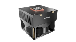
Date Announced: 20 Jul 2009 Nanometrics Incorporated (Nasdaq: NANO), a leading supplier of advanced process control metrology systems used primarily in the manufacturing of semiconductors, solar photovoltaics and high-brightness LEDs, today announced orders for one VerteX™ and multiple RPMBlue™ photoluminescence (PL) mapping metrology systems. The VerteX system is expected to be qualified into a new HB-LED development line, and the RPMBlue systems are expected to be qualified into the high-volume manufacturing line of a different customer. All systems are expected to be qualified in the third quarter of this year.“Our customers are leveraging the increased capability of the VerteX system to address challenges in the rapidly-growing HB-LED market. New end-device deployments in area lighting, LCD back-lighting and an increased understanding of the performance and cost-of-ownership benefits of high-brightness LEDs are driving HB-LED development,” commented Tom Ryan, Director of the Materials Characterization Business Unit at Nanometrics. “Our PL mapping products are well-positioned to support increased development and rapid production ramps as new high-brightness LED manufacturing technologies come online.”The VerteX PL mapping system provides a combination of metrology technologies to support both process development and production control. The VerteX is capable of supporting epitaxial layer metrology on many substrate types and sizes and, due to the illumination system options, can cover the entire spectrum of LED technologies from UV-LEDs through the visible colors to infra-red. Nanometrics’ newest product for HB-LED process control is the RPMBlue. This is targeted at production control of Gallium Nitride (GaN)-based blue HB-LEDs that are increasingly used in LCD back-lighting. The system has been optimized for industry-leading throughput of up to 80 two-inch GaN wafers per hour. Because of the available features and performance, Nanometrics believes its PL mapping systems are used by over 90% of the top-tier HB-LED manufacturers in development and production.About NanometricsNanometrics is a leader in the design, manufacture and marketing of high-performance process control metrology systems used primarily in the manufacturing of semiconductors, solar photovoltaics and high-brightness LEDs, as well as by customers in the silicon wafer and data storage industries. Nanometrics standalone and integrated metrology systems measure various thin film properties, critical dimensions, overlay control, topography, and optical, electrical and material properties, including the structural composition of silicon, compound semiconductor and photovoltaic devices, during various steps of the manufacturing process, from front end of line substrate manufacturing through die preparation for packaging. These systems enable device manufacturers to improve yields, increase productivity and lower their manufacturing costs. The company maintains its headquarters in Milpitas, California, with sales and service offices worldwide. Nanometrics is traded on NASDAQ Global Market under the symbol NANO. Nanometrics’ website is http://www.nanometrics.com.
Contact
Kevin Heidrich 408.545.6000 tel, 408.317.1346 fax
E-mail:[email protected]
Web Site:www.nanometrics.com