NICHOLAS HERRICK and RANJIT PANDHER detail the thermal path that LEDs used in SSL applications follow to ambient and contemplate the advantages of a sintered silver approach for die attachment.
Die attach materials used in the assembly of LEDs directly influence device operating temperatures, and of course we know that heat is the enemy of reliable LED components and finished solid-state lighting (SSL) products. Higher thermally conductive materials, such as sintered nano-silver, allow an LED to operate at lower temperatures. This impact leads to higher luminous flux, efficiency, color stability, and reliability. LED and SSL product developers should fully understand thermal mitigation to yield optimal product performance. Here we will cover research that explains the thermal characterization process that can further guide LED packaging decisions.
Interested in articles & announcements on thermal management and materials for LEDs?
LEDs are predominantly cooled via conduction through the material stack to the heat sink. The die attach layer is one of many layers in the thermal stack, but it can serve as a bottleneck if materials with sufficiently high thermal conductivity aren't used. Typically, 10–30% of the electrical power an LED consumes is radiated as visible light, while the rest is released as heat. This heat predominantly leaves the LED via conduction through the die attach layer stack.
The most common industry evaluation of LED thermal behavior is the junction-to-ambient thermal resistance. In this test, the whole LED stack is measured at once, with no differentiation between various component layers. This method is sensitive to variations in the die, package layers, thermal interface material (TIM), and heat sink. In this article, we outline a method to measure the high thermal conductivity of a sintered-silver die attach layer.
LED assembly — Dies and packages
LEDs are most commonly packaged for ease of assembly into SSL products. LED chips are adhered to a substrate with a die attach material. The die attach material forms an important link in the thermal path of the LED to ambient. In many cases, the die attach material also forms the electrical connections. An LED chip affixed directly to a metal substrate is an example of chip-on-board (COB) architecture and is common in high-power LED designs. Heat generated at the LED junction conducts through the stack layers to reach the heat sink. These layers include the chip, die attach layer (Level 1), package substrate, package attach layer (Level 2), dielectric, and metal substrate.
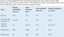
The layered structure of a single COB LED stack can be considered one-dimensional from the p-n junction through the die attach layer. After heat enters the metal substrate, it can spread in-plane before it is conducted to the heat sink and then to ambient. Therefore, because of the small cross-sectional area of the one-dimensional stack, each layer needs to be highly thermally conductive (or, equivalently, have low thermal resistance; see Table 2). As we will detail shortly, the dielectric layer in a typical stack dominates the total thermal resistance of a packaged LED. For the experiment we will discuss here, we mounted LED chips with a die attach layer directly to copper pedestals in what is called an active substrate with no dielectric layer, which as you will see enabled high-sensitivity measurements.
The LEDs used for this experiment were based on aluminum gallium indium phosphide (AlGaInP) layers on silicon (Si) substrates. They were 1×1 mm in footprint and 225-μm thick. The typical operating current for the LEDs is 350 mA with a forward voltage of 2.4V. The peak wavelength is 624 nm.
Die attach materials
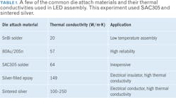
In this study, we sought to develop a test method to understand the influence of the die attach layer on the thermal performance of high-power LEDs. Die attach materials vary widely in their thermal performance, price, and intended applications (Table 1). We compared two die attach materials: a mid-performance, industry-standard solder alloy (SAC305) and a high-performance alternative (sintered nano-silver paste).
SAC305 is an electronics industry-standard, lead-free solder alloy composed of 96.5% tin, 3.0% silver, and 0.5% copper. The purpose of SAC305 in this experiment was to function as the control as we investigated the unknown in-situ thermal conductivity of sintered nano-silver.
The sintered nano-silver paste used here is designed for pressure-less die attach assembly and uses typical SMD (surface-mount device) manufacturing processes such as printing or dispensing and pick-and-place. It must, however, be sintered at high temperature in an oven.
The thermal conductivity of bulk silver is 429 W/mK, but because of nano-pores the expected thermal conductivity of sintered nano-silver is lower. Laser-flash thermal conductivity measurements of bulk sintered silver samples are >200 W/mK.
Measuring the thermal conductivity of sintered nano-silver layers is challenging because of their high thermal conductivity. The microscopic porosity of sintered materials is highly dependent on sintering conditions, such as pressure, temperature, and duration. Because of this, measurements done on a large sample are not representative of thin die attach layers in an LED assembly. Therefore, sintered silver LED applications packages must be evaluated in situ, i.e., by attaching an LED die to a substrate.
The thickness of the die attach layer, also referred to as the bond line thickness (BLT), is a key property of an LED assembly. Thicker BLTs relieve thermal stresses, but contribute to higher overall thermal resistance. We measured the BLT of our LEDs via a vertical measuring microscope with follow-up cross sectioning to confirm the results.
Substrate and dielectric
LED COB substrates are typically made of copper or aluminum. These high-conductivity metals allow heat to spread before it enters the TIM and the heat sink. However, most LED substrates have a dielectric layer between the die attach pad and the metal core. This layer has comparatively high thermal resistance — so much so that the total thermal resistance of the LED stack is overwhelmingly dominated by the thermal resistance of the dielectric layer (Table 2).
In our experiment, we needed to measure the very small thermal resistance of sintered silver. With the dielectric layer present, the thermal resistance of a sintered silver layer was only 0.8% of the total thermal resistance, making accurate measurement impossible. Solder die attach layers comprise only 2.7% of the total thermal resistance when a dielectric is present, making these measurements challenging but possible.
Removing the dielectric gives a direct heat path to the metal substrate and vastly decreases junction-to-ambient thermal resistance. Without a dielectric, the sintered silver die attach layer's contribution is 8.4% of the total stack resistance and solder's contribution is 21.3%. This ten-fold increase makes the measurement possible with commercial off-the-shelf hardware.
Thermal measurements
The test we performed is based on JEDEC Standard EIA/JESD51-1 "Integrated Circuits Thermal Measurement Method Electrical Test Method (Single Semiconductor Device)," 1995. Because the forward voltage of a diode varies with the temperature of the p-n junction, it can be used as a temperature sensor. Also, LEDs generate significant heat when they are operated at high power, so they can also be used as heaters. To use an LED as a temperature sensor, it should be operated at very low current so that there is no internal heating. By rapidly switching between high and low currents, we can utilize LEDs as test devices to measure the thermal resistance of all the layers in the die attach stack. If the switch between heating and sensing currents happens fast enough, then the sensing current can be used to measure the temperature of the previous heating phase.
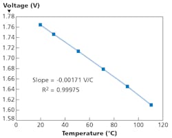
Using an LED as a temperature sensor requires calibration, i.e., we need to determine its temperature sensitive parameter. The temperature sensitive parameter of an LED, also known as the k-factor, is a linear relationship between the forward voltage of the LED and the junction temperature. Fig. 1 shows a plot of forward voltage as a function of the temperature for a typical LED used in our experiment. The slope of the line is the k-factor, measured in volts/degree Celsius. The LEDs in this study had measured k-factors of 0.00171 V/°C.
LED heating transient
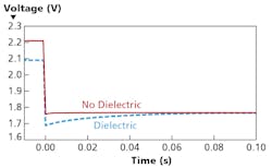
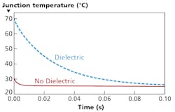
Fig. 2 shows the voltage of an LED when it rapidly switches from high to low current. In this case, the LED was operating at 0.7A for long enough to thermally stabilize, then switched to 0.01A. At the moment of switching (t=0), there is a transient event in which the voltage rises quickly because the LED begins to cool after the current switches. As the LED temperature approaches the heat sink temperature, the voltage stabilizes at the reference voltage. Using the temperature sensitive parameter we can calculate the junction temperature of the LED during this time (Fig. 3). If the power supply switches sufficiently fast, then the voltage immediately after the switch will correspond to the temperature of the LED when it was operating at the heating current.
The duration of the transient voltage response is proportional to the total thermal resistance of the LED assembly, while the amplitude is proportional to the highest temperature the LED sees during its heating phase. Therefore, a substrate with a dielectric will have a longer duration and higher amplitude transient than a dielectric-less substrate. A shorter-duration transient is the downside of removing the dielectric and necessitates a fast switching and high-resolution power supply. The transient duration for LEDs assembled on dielectric substrates was around 50 ms, while LEDs assembled on dielectric-less substrates were less than 10 ms.
In our experiment, we used a source measurement unit capable of switching currents in under 30 μs. The current and voltage were monitored at 10 kS/s (kilo-samples per second) during switching. By acquiring the electrical data at high speed, we avoided the need to extrapolate voltage data to t=0.
Junction temperature
The junction temperature (Tj) of an LED is the temperature at the p-n junction where light is generated. It is the chief contributor to the total lifetime of the LED and influences the LED's color, total luminous flux, and efficiency.
The following equation, referred to as the forward voltage shift method, can be used to measure Tj during LED operation:
Where:
VR is the reference voltage of the LED when the current is below the self-heating threshold (measuring current) and the LED is at THS temperature.
VS is the sensing voltage of the LED immediately after switching from heating to sensing current.
k is the temperature sensitive parameter in units of volts/degree Celsius.
THS is the temperature of the heat sink in Celsius.
Thermal resistance calculation
The thermal resistance of the LED package can be calculated by knowing the junction temperature of the LED at several operating currents:
Tj = Rth . Ph+ THS
Where:
Tj is the junction temperature, which is a function of heating power, Ph.
Ph is the heating power of the LED (see equation below).
Rth is the thermal resistance of the LED assembly, in °C/W (or equivalently, K/W).
THS is the temperature of the heat sink, in Celsius.
We are focused on the heating power of the LED versus the electrical power, because some of the electrical power is converted into light. Heating power, therefore, is defined as:
Ph = PE – Po
Where:
Ph is the heating power of the LED, in watts.
PE is the electrical power of the LED, in watts.
P0 is the optical power of the LED measured in an integrating sphere, in watts.
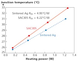
Using the equations above, we can plot junction temperature versus heating power (Fig. 4). The slope of the line is the total thermal resistance of the LED package, in units of °C/W.
Thermal conductivity
By assembling LEDs identically except for the bond line thickness (BLT), we formed an experiment in which BLT was the independent variable and thermal resistance the dependent variable. Using this method, we measured the thermal conductivity of the die attach material:
Rth = RS . Th+ RRem
Where:
Rth is the total thermal resistance of the LED package, which is a function of Th.
RS is the thickness of the die attach layer (BLT).
Th is the scaled thermal resistance of the die attach layer, measured in (K/W.m).
RREM is the thermal resistance remnant. It corresponds to the y-intercept of this linear equation, meaning it is the theoretical thermal resistance of the package if the BLT = 0. In other words, it is the thermal resistance of all the non-die attach layers.
Once the scaled thermal resistance, RS, is known then the thermal conductivity of the material can be calculated:
Where:
k is the thermal conductivity of the die attach material, in W/m-K.
A is the surface area of the die attach layer.
The thermal resistance remnant RREMmerits additional discussion — it is the total resistance of all the in-common elements of the LEDs tested, including the resistance of the die, boundary layers of the die attach material, dielectric (if present), substrate, TIM, and heat sink. The die attach boundary layers have different resistance properties than the bulk die attach material because, in the case of sintered silver, the material makes imperfect physical contact with the adjacent surfaces or, in the case of solder, there exists an alloy gradient at the interface. However, by varying only the BLT of a die attach material we can discount all the other resistance layers, thereby measuring the bulk conductivity of the material in situ.
Results
Twenty-seven LEDs were assembled with sintered silver covering a BLT range of 10–160 μm. These were sintered for 1.5 hours at 225°C. Twenty LEDs were assembled with SAC305 preforms to achieve a BLT range of 18–133 μm. These were reflowed in vacuum to minimize voiding. Two wirebonds were used on each LED. Voids were measured and only samples with percentages less than 10% were used in the study. For testing, each LED was mounted to a thermoelectric cooler set to 25°C with a layer of indium to act as a TIM.
For every measurement, the LED was required to thermally stabilize to within 0.02°C of the set temperature for at least 10 seconds. Each LED was powered via constant current at 0.1, 0.3, 0.5, and 0.7A and the junction temperature was measured. The optical power of every LED was measured in an integrating sphere to calculate each sample's thermal power at each current.
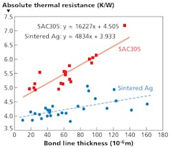
Junction temperature measurements gave a scaled Rth of 4834 K/Wm for sintered silver samples (Fig. 5). This corresponds to a thermal conductivity of 206.8 W/mK. LEDs assembled with SAC305 showed a scaled Rth of 16,227 K/Wm and corresponding 61.6 W/mK thermal conductivity.
The y-intercepts of the fitted lines in Fig. 5 indicate that sintered silver has slightly lower interfacial resistance than SAC305. This is likely due to interfacial inter-metallic compounds and voids in SAC305 (despite significant efforts to minimize them). The unavoidable existence of voids in solder assemblies (even when using preforms and reflowing in vacuum), versus near void-less sintered silver performance, is a significant drawback.
The purpose of this experiment was to measure the thermal conductivity of sintered silver in-situ. In order to verify the accuracy of the method, we also measured SAC305. Therefore, if our measurement results for SAC305 were accurate, then we have some assurance that our measurements of sintered silver are also accurate. The results are encouraging because they accurately measure the thermal conductivity of SAC305 at 61.6 W/mK, which is known to be 64 W/mK. Our results are within 10% of the published value. We can therefore state with confidence that the bulk, in-situ thermal conductivity of Alpha sintered silver paste is within 10% of 206.8 W/mK.
Conclusion
The die attach layer is an essential heat conduction layer in an LED assembly and its performance strongly depends on thermal conductivity. While JESD51-1 is the standard for determining the total thermal resistance of an LED assembly, we adapted it to measure the bulk thermal conductivity of high-performance sintered silver. By assembling test samples without dielectric and using sufficient power switching, we measured the thermal conductivity of our sintered silver material and compared it to SAC305. Sintered silver die attach materials offer excellent thermal performance improvements versus SAC305 solder.
NICHOLAS HERRICK and RANJIT PANDHER represent Alpha Assembly Solutions.

