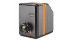
MicroSense has introduced and shipped a new, next-generation automated sapphire wafer metrology tool, the MicroSense UltraMap C200. Designed specifically for high throughput dimensional measurement of sapphire wafers for LED manufacturing, the UltraMap C200 provides throughput of ninety 6" diameter sapphire wafers per hour with lowest cost of ownership (CoO). The UltraMap C200 utilizes MicroSense's novel two sided capacitive sensing technology to measure sapphire wafer geometry including thickness, TTV (total thickness variation), bow, warp, and LTV (local site thickness variation).
In order to improve sapphire wafer yields and drive down wafer cost, wafer manufacturers need to measure at more steps in the wafering process. Unlike metrology tools based on optical methods, the MicroSense UltraMap C200 measures sapphire wafers and substrates with any surface finish -- as cut, lapped, ground, polished, textured and patterned sapphire substrates (PSS) -- without sacrificing wafer throughput or measurement repeatability. Wafer surface condition has no effect on measurement performance.
The UltraMap C200 is available in three versions including tools with robotic loading, robotic loading with cassette sorting and a bench top tool. The UltraMap C200 handles wafers ranging from 2" to 8" in diameter.
Contact:
David Kallus, Director of Dimensional Metrology - MicroSense
+1-978-212-3275
E-mail:
Web site:
www.microsense.net/products-wafer-metrology.htm
Submit new products, case studies/projects, and other press releases at http://www.ledsmagazine.com/content/leds/en/addcontent.html and http://www.ledsmagazine.com/content/leds/en/iif/add.html.