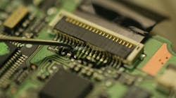
Date Announced: 10 Sep 2013 Bruker introduces new LumiMap electroluminescence tool for optical and electrical characterization on epi wafers for HB-LEDsNew technology delivers fast and repeatable measurements for epi process quality controlSHENZHEN, China - At 15th China International Optoelectronic Exposition (CIOE 2013), Bruker introduced the new LumiMap™ Electroluminescence System for uncompromised HB-LED epi wafer process metrology. LumiMap joins a suite of other successful Bruker HB-LED epi metrology tools, and it incorporates many of the advanced features of Bruker’s flagship metrology products. Proprietary, patent-pending features of the new system include the durable conducting probe, a unique wafer edge contact solution, and advanced I-V curve modeling for accurate and repeatable forward voltage value measurement. These features enable LumiMap to deliver the most accurate and repeatable forward and reverse IV characteristics, spectral intensity, wavelength and spectral width measurements on 2- to 6-inch epi wafers, with a wide range of current settings.“LumiMap provides more accurate and reliable electrical and optical epi wafer measurements than the traditional indium dot method,” said Dr. Ryan Lee, executive VP and CTO of Foshan Nationstar Optoelectronics Co. Ltd. “A reliable electro-luminescence quality check immediately after MOCVD will help us further improve epi wafer yield and reduce costs.”“Bruker is pleased to bring a new technology solution to HB-LED manufacturing, rounding out our other HB-LED metrology technologies in 3D optical microscopy, atomic force microscopy and XRD/XRF for PSS wafers and epi wafer multi-quantum layer characterization,” said Dr. Xiaomei Li, vice president of segment marketing of the Bruker Nano Surfaces division. “LumiMap ideally serves stringent HB-LED manufacturing cost reduction goals at a time when the industry is poised for unprecedented growth.”“LumiMap electroluminescence technology fills the current lack of fast, non-destructive, reliable and repeatable optical and electrical measurement solutions to improve epi wafer yield and LED device quality at the epi wafer stage,” added Robert M. Loiterman, executive vice president and general manager of Bruker’s Stylus and Optical Metrology Business. “With LumiMap, the HB-LED industry can now get accurate electrical and optical feedback in minutes rather than days, reducing scrap events and operating costs.”About LumiMapLumiMap is a value-oriented alternative to conventional, multistep, operator-dependent indium dot methods of epi (made by epitaxial growth) wafer characterization. The system features rapid, non-destructive, no post measurement chemical cleaning, software-controlled measurement locations, and repeatable optical and electrical measurement capabilities through forming a temporary LED (light-emitting diode) device on an epi wafer. The results obtained by LumiMap are well correlated with those on the final HB-LED (high brightness LED) device, providing an early warning of process shifts, which in turn reduces the risk of expensive scrap events and improves yields. Simple wafer exchange and intuitive software provides the industry’s easiest to use interface for production quality control, as well as epi process development. The long measurement lifetime of the proprietary conducting probe meets the strictest industry cost of ownership requirements.About Bruker Corporation (NASDAQ: BRKR)Bruker is a leading provider of high-performance scientific instruments and solutions for molecular and materials research, as well as for diagnostics, industrial and applied analysis.
Contact
Stephen Hopkins, marketing communications, Bruker Nano Surfaces 520-741-1044 x1022
E-mail:[email protected]
Web Site:www.bruker.com