Flip-chip LED architecture promises to pervade the packaged component space, and JULIAN CAREY explains how the sapphire-up design can combine with new phosphor technologies to increase light quality and lower costs.
Over the last year, we have definitely seen the levels of solid-state lighting (SSL) adoption increasing with widespread installations, as industry analysts have been predicting for several years now. We are seeing installations ranging from street lighting to parking garages, from expanded uses in retail and hospitality applications to commercial and industrial applications. The technologies being incorporated, the applications, and the range of installations are growing dramatically. Still, light quality and component cost remain issues for the LED industry, and new chip architectures and phosphor-application techniques can deliver benefits in both regards.
Indeed, the increased demand for SSL is pressuring the industry to simultaneously improve quality, lower costs, and reduce manufacturing complexity throughout the supply chain. In response to these pressures, new LED manufacturing technologies are being developed across the full range of chip fabrication techniques, starting with a new generation of semiconductor capital equipment, improved process engineering, and the development of advanced materials. In this vein, Intematix is focused on engineering more rugged and efficient phosphor materials, as well as phosphor-application schemes, to reduce manufacturing cost and complexity while improving light quality.
Phosphor pre-formed films
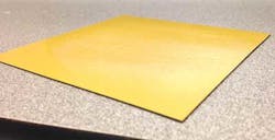
In one innovative example of new technologies, phosphors are being manufactured into pre-formed polymer film sheets or glass tiles. We will even study the use of optical-ceramic materials that may be applied directly onto the light-emitting surface of LED chips. The promise of these novel manufacturing technologies is to eventually enable wafer-level packaging (WLP) of LED chips. WLP promises to lower chip manufacturing costs by eliminating redundant packaging steps while simultaneously improving LED chip efficacy, reliability, and quality. Ultimately, these technologies, combined with improved manufacturing systems and processes, could lead to the elimination of binning - producing white LED chips with a performance variance within 2 SDCM (standard deviation of color matching or a two-step MacAdam ellipse).
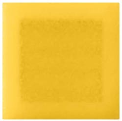
Still in development, these manufacturing techniques are currently being tested on flip-chip LED architectures, where both positive and negative contacts are on the bottom of the chip. Fig. 1 depicts a Samsung flip-chip LED with a uniform light-emitting surface. Samsung announced the architecture in a keynote address at the Strategies in Light 2014 conference.
Indeed, the flip-chip approach enables a more planar light-emitting surface than the typical wire-bonded lateral chip architecture, providing an easier implementation of the new phosphor-application technique. Furthermore, flip chips are becoming more common in the industry, as even second-tier manufacturing companies have caught on to the benefits they provide and have thus increased their flip-chip manufacturing.
WLP with flip-chip architectures
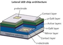
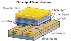
The most prevalent LED chip architecture in the SSL technology sector today remains the so-called lateral chip structure in which the substrate is at the bottom of the material layer stack that comprises the LED (Fig. 2). Flip chips have many advantages in simplifying design and manufacturing. First, since the electrical contacts are on the bottom, there is no need for the wire-bonds that are required to connect with the electrical contacts on the top of a lateral LED (Fig. 3). This means that you can eliminate a full step in the manufacturing process. Furthermore, wires as a potential failure point are no longer a concern.
Flip chips also improve chip efficiency. With the electrical contacts out of the way, more of the chip surface is available to emit light. The entire chip surface becomes a "window" into the light.
This window allows the phosphor materials to be laid right over the top of the chip. The full planar surface of the chip is thus available. At this point, you can apply the phosphor material either at the packaging step in LED manufacturing or at the wafer level - or perhaps somewhere in between.
With flip-chip architecture, phosphor pre-forms, manufactured in large polymer or glass sheets or ceramic platelets, can be precisely targeted to uniformity standards within 1 SDCM. Moreover, such phosphors can be applied to LED chips in two different ways as mentioned before (Fig. 4).
In the first method, the pre-formed phosphor can be applied at the wafer level. During the manufacturing of LED wafers, all of the individual LED chips are attached to one another on the wafer. Before singulating the die (i.e., sawing the wafer into individual chips), a film, glass, or ceramic phosphor pre-form is placed on the top of the entire wafer. This creates a sort of phosphor "hat" on each chip. The wafer is then sawed into individual LED chips with the phosphor on top, thus creating what some call an LED "white" chip. The LED has a minimal package and a white reflective coating is applied to the sides of the structure to maximize light extraction.
Binning requirements
This WLP technique offers many benefits beyond the typical emitter or chip-on-board (COB) packaging available today. Bulk processing is moving in this direction for efficacy, uniformity, and low cost. This technique will ideally take the industry to new manufacturing efficiency levels, whereby binning is greatly reduced or no longer needed.
Binning is currently required since each LED wafer typically has areas of wavelength nonuniformity. LED manufacturers sort their production of LED chips by various wavelength bins, allowing light source manufacturers to select only those LEDs that meet their acceptable performance ranges while maximizing the overall manufacturing yield and usage of each of the bin ranges. Binning is a time-consuming, costly, and inefficient process. As the next generation of metal organic chemical-vapor deposition (MOCVD) reactors — critical to LED formation — comes on line, offering improved within-wafer and wafer-to-wafer wavelength uniformity, binning may be greatly reduced.
To reach this market ideal, manufacturers would start out with a uniform blue LED wafer with a wavelength uniformity between 2 and 2.5 nm in wavelength, or 1 SDCM as converted through the phosphor. A phosphor film that is also uniform to 1 SDCM is laid over the entire wafer, which is then diced up into individual LED chips. With this process, every chip matches each other within 2 SDCM. There would be no need to sort the chips further, since each one is essentially uniform. While this process creates a path to this industry goal, the technology must still make substantial progress before we can claim to have achieved it.
Use of phosphor pre-forms post-singulation
A second way that phosphor pre-form can be applied is after the wafer has been singulated. Actual wafers don't necessarily have perfect wavelength uniformity; instead, there are various zones wherein the chips will be a few nanometers off from the desired wavelength. A couple of processing choices can be made at this point. The phosphor can be applied to the entire wafer, as described previously, or the individual LEDs can be sub-binned. When the wafer is singulated, individual chips are tested and sorted by wavelength, and then they're picked and placed into bin-tiles of chips of the same wavelength. This basically creates a new wafer, based on the test data from individual chips, and a uniform bin tile.
Once the wafer has been divided and the LED chips are virtually transferred to their appropriate bin tiles, the phosphor pre-form may then be sawed into pieces that perfectly match the size of the LED chips on the bin-tile. The segmented pre-forms can then be applied to the appropriately matched bin tile, producing highly uniform, 2-SDCM white LED chips while eliminating the cost of conventional packaging techniques.
The pick-and-place bin-tile process enables greater efficiency, reduces binning, and lowers costs. However, this can actually be disadvantageous to manufacturers. Since phosphor is sensitive to certain wavelengths, manufacturers will be forced to increase their inventory of pre-formed phosphor sheets to match the typical range of chip wavelengths. With current manufacturing processes, LED packaging companies store the phosphor materials, which are then mixed differently for each bin tile. In the wafer-level application, companies only need one film that delivers the desired color. Yet this pick-and-place application process forces companies to store frozen pre-formed films for each color that match the different bin tiles, thus creating an explosion of products. Storage logistics are one technical detail that will need to be addressed as this process moves forward.
This is where it becomes obvious that the front-end of line (FEOL) improvements mentioned at the beginning of this article can have a big impact. As within-wafer and wafer-to-wafer uniformities become better, reliance upon pick-and-place methods can be greatly reduced. Manufacturers will be able to reduce their SKUs (stock keeping units). Moreover, manufacturing complexity throughout the supply chain will be reduced and prices will come down.
Polymer versus glass phosphor pre-forms
As mentioned previously, phosphor pre-forms are being developed in both film and glass. The film is a polymer carrier, and in Intematix's case an outgrowth of the company's remote phosphor development effort, which gave the company the technology and capacity to develop these pre-formed phosphor solutions. These films, or glass pre-forms, can be manufactured with various phosphor recipes to produce a customer's required quality of light at a given chip wavelength.
Glass pre-forms, however, are more of a manufacturing challenge. Integrating the phosphor material into glass is inherently more difficult than with polymer film and will require more development work. Yet glass provides a higher refractive index, offering greater efficiency and giving the chips and SSL package another efficacy boost. Intematix believes that the industry could see phosphor pre-form manufacturing using the phosphor polymer film carrier technique by the end of 2014. Manufacturing with the glass pre-form will take a little longer, but we could begin to see it used by early 2015 for flip-chip architectures only.
Optical ceramic phosphor converters
As we have established, optical ceramic phosphor materials represent a third technical approach for the application of phosphor materials directly onto the light-emitting surface of LED chips. Different than polymer or glass pre-forms, it offers significant advantages for high flux-density applications such as spotlighting, projection, and automotive headlights.
Optical ceramic converters offer several thermal advantages. First, these materials have much higher thermal conductivity, allowing for faster thermal dissipation. The resulting lower operating temperature typically produces greater conversion efficiency for the light source. SSL light sources using this technology can offer greater energy efficiency or will allow for the LED chips to be driven at higher current densities for greater light output. These same properties also give the light source much greater thermal stability over time, hence greater system reliability. The overall lower operating temperature means that the phosphor materials are much less likely to experience thermal damage or to "brown," especially in high flux-density applications.
Ceramic converter material can be made in yellow, green, and white emission. Since the white color coordinates are within European Commission for Europe (ECE) specification for headlights, ceramic materials are good applications for automobiles, according to Schott, a global manufacturer of special glass and specialty materials.
Currently, the biggest disadvantage for ceramic phosphors is their higher cost. To date, a limited number of chemical systems have been explored and developed as ceramics. Additionally, ceramic processing steps beyond making the powder are required in ceramic phosphors, which are not necessary for glass and film phosphors. Due to these additional steps, manufacturers must invest in ceramic processing equipment, which drives up the manufacturing costs. In the near future, due to this higher cost differential, it is unlikely that optical ceramic phosphor materials will be used in any but the most heat-sensitive or high flux-density applications such as automobile headlights where the distinct advantages of this technology outweigh the cost considerations.
Polymer pre-forms with wire-bonded chips
Intematix also believes that, despite the advantages, flip-chip production will represent only about 25% of the market in 2015 as the technology matures. This means that 75% of the market will continue to comprise lateral chips or chips using wire-bonding techniques. This large segment of the market shouldn't be ignored, as there are possibilities that the polymer film approach could work with wire-bonded LEDs if it is laminated onto the chip. Such a scenario would require that the chip already be wire bonded and working, then the polymer would be applied over it. The material would need to be in a soft gel phase such that the wire bonds would remain as they are and not be disturbed. As the technology continues to evolve, Intematix's goal is to extend the approach beyond flip-chip architectures to include wire-bonded chips, as well.
Overall, Intematix believes that these new manufacturing technologies hold great promise to reduce manufacturing costs, improve light quality, and provide greater efficiency while simultaneously offering reduced binning - ultimately driving toward simplification of the LED light source manufacturing process.
JULIAN CAREY is the senior director of marketing for LED phosphors at Intematix Corp.


