This article was published in the June 2013 issue of LEDs Magazine.
View the Table of Contents and download the PDF file of the complete June 2013 issue, or view the E-zine version in your browser.
+++++
Producers of LEDs and solid-state lighting (SSL) have made stunning progress in technology to improve efficiency and lower cost, but there's still plenty of room for improvement in this young sector to help propel wider adoption. Indeed, LED manufacturers are constantly striving to optimize manufacturing processes both to bring down costs and improve performance. Some researchers now say the next significant opportunities may be in adding new functionalities through on-chip integration of features and in simplifying the supply chain. More disruptive technologies like gallium-nitride-on-silicon (GaN-on-Si) manufacturing and quantum dots could be close to the tipping point for adoption, while nanowire alternatives remain potential game changers further down the road.
Several of the speakers that will participate in a Semicon West (July 8-11, San Francisco) session entitled, "Looking ahead to the next generation of HB LED manufacturing technology," spoke out about their views on next steps for the industry. Opinions vary greatly, although there is already evidence of broader functionality at both component and system level. Conversely, significant questions remain about fundamental changes to the LED in terms of materials such as silicon, nano technology, or even quantum dots as replacement for phosphor.
More functions for SSL
“What's driving the market now — and what I think will increasingly dominate the technology innovation in LEDs in the future — is new functionalities,” suggests Wouter Soer, senior researcher at Philips Lumileds. He sees new functionalities emerging at both the component and system level.
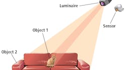
At the system level, Soer points to Philips' recent introduction of what may be the first software development kit (SDK) for light bulbs. The SDK and published application programming interfaces for Philips' Hue bulb simplify development of iPhone and Android apps for controlling the color-tunable lamps. The lamps integrate ZigBee wireless connectivity and memory. Even before the release of the open platform, users were already hacking into the bulb to control the brightness and color of lights throughout the house, to flash colors in sync to music, or to match the lighting inside with the daylight outside with smart phone programs. Philips wants to open up the capability for more users to interact with the light, says Soer.
Simplifying the supply chain
Perhaps a more subtle area of technological change that could also have big impact on the LED sector is re-thinking systems component capabilities to simplify the supply chain. The tremendous diversity of the LED market across different applications, with its large number of components and product variations, must be managed by all players across the supply chain and presents a big challenge for the industry.
One solution may be to optimize across the whole system instead of thinking separately in terms of chip, package, module, and luminaire. One approach Lumileds is developing in a DOE-funded project is a hybrid module, which adds red LEDs to deliver warmer color temperature lighting. That concept is not new, but approaching it at a modular level will enable more SSL manufacturers to utilize it because mixing colors precisely with multiple channels of LEDs is a complex problem.
Indeed Lumileds' project involves integrating more electronic controls at the module level to simplify the need for them later in the supply chain. This not only can simplify what's needed from the driver — or ultimately even include the driver itself — but also can simplify the value chain, which allows the lamp maker to just plug in the part and not have to test it again. “If we partition the system in the right way, everyone will have to deal with fewer SKUs, which will reduce costs,” maintains Soer.
GaN on silicon
Moving on to LED manufacturing and materials, GaN-on-Si technology has been a hot topic. Proponents believe it can deliver lower LED cost because silicon wafers cost less than the sapphire wafers that are most widely used today. Moreover, once the epitaxial process is complete, manufacturers can use existing IC fabs and automated tools to handle the back end of the production process.
“There's no answer yet about GaN on silicon, but there will probably be one within the next 12 to 18 months,” suggests Eric Virey, senior analyst for LEDs at Yole Développement. “It depends a lot on how successful Bridgelux and Toshiba are.”
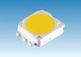
LEDs Magazine has closely followed the progress of the duo. Toshiba announced production start last December and released the detailed specs of its silicon-based LEDs (Fig. 2) in January. Bridgelux has since sold its silicon-centric intellectual property to Toshiba, although the company still has an agreement to buy Toshiba LEDs.Virey believs that if the Toshiba GaN-on-Si product proves extremely competitive in cost and performance, many of the other big players, who all have research programs, will follow. However, if the lower costs don't turn out to be significant enough to counter the likely somewhat lower performance, others will likely back off their efforts. The most likely scenario, argues Virey, will be somewhere in the middle, with GaN-on-Si adopted by some companies who have the silicon experience and the depreciated silicon fabs that make it most cost effective, and for some applications best suited to its cost and performance.
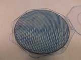
GaN-on-silicon wafer supplier Azzurro argues that the quality of LED devices made on silicon could be just as good with costs significantly lower – which could potentially mean big changes for the LED industry. The company sells 150-mm (6-in) and 200-mm (8-in) silicon template wafers with the buffer layers grown, ready for LED makers to grow their own light-emitting epitaxial structures on top, almost as usual, then finish processing on a standard silicon line (Fig. 3).
Azzurro reports that it is now qualifying template wafers at its fab in Germany for customers who can start testing the process with 2-in template wafers. Epistar has reportedly ported its structures to the 150-mm template wafers. Wafer volume is also supported by demand from users making power semiconductors, where the GaN-on-Si technology has the added pull of a big gain in performance for most applications.Azzurro co-founder and executive vice president of business development Alexander Loesing says the company inserts strain-engineering layers into its buffer stack to control the degree of bow after growth. The methodology also allows growth of a thicker GaN layer than most of the other buffer-layer technologies, which helps for making higher quality LEDs. After epitaxial growth, the excess silicon is thinned away with standard low cost removal processes, leaving wafers with the standard thickness and flatness required for processing on a standard silicon line.
“The strain-engineered wafers allow more homogenous processing for better control of wavelength, output power and forward voltage,” claims Loesing. “Silicon actually has better thermal properties that can improve the temperature homogeneity across the wafer for more uniform epi growth, for tighter binning, though controlling bow during growth helps as well.” The better yields and higher throughputs of the production workhorse 150-mm and 200-mm generation of silicon tools could reduce LED production costs – especially if companies don't have to invest in the equipment because they have their own depreciated fab already or can find a foundry to do the processing.
Azzurro argues that even when demand picks up enough to require the additional capacity, the economics of converting to 6-in sapphire wafers will be marginal for many companies because of the higher cost of the larger sapphire wafers and the technical challenges of more strain and bow across their larger area as well. Thus, switching to larger diameter GaN-on-Si template wafers with CMOS-foundry post-epi processing could be the more appealing path to staying competitive for many companies. “If someone comes in with GaN on silicon that's competitive in performance, then the price advantage will be compelling,” says Loesing.
Nanotech and quantum dots
“Nanowires could also be a big game changer further out,” suggests Virey. “The industry has done pretty well in already harvesting much of the low hanging fruit with the current conventional technology.” While research results from these nano column structures for the light extraction surface or the light emitters are impressive and have garnered significant venture capital funding from respectable firms, the key will of course be how successful they are in scaling to volume manufacturability. The novel structures must be grown homogeneously across the entire 6 or 8-inch wafer surface and will need a process that is as compatible as possible with the standard semiconductor tool set for likely commercial volume manufacture, he notes.
“Quantum dots have been promising for the last 10 years, but they may now be at a tipping point,” says Virey, now that the technology is in some of the first commercial products, such as the Sony television using QD Vision's quantum dots. The technology has significant potential for improving color and reducing energy consumption using blue instead of white LEDs and converting the color by a sheet of encapsulant with embedded dots. Big TV makers seem convinced they can be manufactured at a reasonable cost since many are collaborating with the startup suppliers.
In SSL applications, quantum dots could be an effective replacement for phosphor because the technology exhibits much tighter spectrum control. For example, red phosphors inherently generate energy beyond the human visual sensitivity range, but red quantum dots could eliminate that wasted energy.
GaN-on-GaN LEDs and native GaN substrates, meanwhile, could offer better performance at high current density. Soraa is the only player in that segment at the moment. The homogeneous technology will likely find application where high density light per surface area is needed, such as in MR-16 lamps and also in projection and automobile headlights, and more, as costs come down.


