This article was published in the March 2013 issue of LEDs Magazine.
View the Table of Contents and download the PDF file of the complete March 2013 issue, or view the E-zine version in your browser.
+++++
LEDs are becoming increasingly popular in lighting applications due to energy efficiency and long life, but the industry is still learning how to deliver optimum system performance in solid-state lighting (SSL) products. The shape of traditional LEDs poses one challenge. While many LEDs appear round because of the primary optic installed over the emitter, the actual source has typically been rectangular or square. Round sources, however, can provide increased efficacy, better uniformity, and superior light quality in many applications.
The COBs are often referred to as LED packages with the industry not differentiating multi-emitter products. Indeed, that label is used in square packages as well. While analysts and others in the industry equate single and multi-die packages, for instance in terms of units sold, the SSL product developer must understand the difference.
It may not be readily apparent to the end user, but the architectural distinction is important as it has major system implications. Although the COB arrays can create a reasonable approximation of a round source with an appropriate amount of illumination, the lumen density (lumens/mm2) is low due to the space left between die for interconnects and to comply with layout design rules.
Lumen density
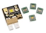
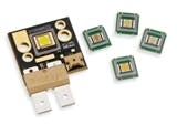
For example, a typical COB array might generate 1000 lm over a source area of 100 mm2 for a lumen density of 10 lm/mm2. By contrast, Luminus Devices has created a single LED chip with conformal phosphor coating that emits directly from the epitaxial material in a round shape (Fig. 1). The result is significantly higher lumen density. Luminus' CBT-140 round LED emits up to 4200 lm from a source area of 14 mm2, resulting in a lumen density of 300 lm/mm2.
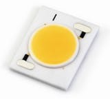
Monolithic round LEDs have a lumen density that is approximately 30× greater than typical COB arrays with circular emission. On the other hand, there are COB LEDs (Fig. 2) that offer greater lumen output than what you get in single die products. At the extreme end of the spectrum, Sharp recently announced a 100W COB LED that tops out at 14,000 lm. More typically the Sharp Mini Zenigata COB LEDs measure 15×12 mm and range in output to more than 1000 lm (Fig. 2).
Until recently, any LED fixture of modest output consisted of as many individually packaged LEDs as were necessary to produce the requisite flux. This approach enabled street lights, down lights and such, but could not be used for products like profile spots. The concept of developing and manufacturing an LED with a circular emission area becomes compelling only when it's possible to fabricate an individual chip with substantial output in the range of thousands of lumens.
Such a higher lumen output enables a single source with a very simple, compact and efficient optical system to create a light engine for a particular fixture. In scaling up to applications that still cannot be served by a single source, much of the round source efficiency advantage can be preserved using architectures that combine a modest number of LEDs thereby enabling fixtures with 10,000 to 20,000 lumen system output or even higher.
Limited étendue systems
Lumen density becomes critical in enabling high lumen systems that are optically constrained, otherwise known as étendue limited. Étendue is the product of a source's or optical system's area and angle. It is an optical conservation law that no optical system can reduce étendue, it can at best preserve it and generally increases it.
Luminus Devices has excelled as a manufacturer of LEDs forétendue limited applications, most notably for DLP and LCD digital projectors of various sizes. It is worth noting that these systems exploit the very same geometric concept as the new round LEDs – they match the shape of the source to that of the system aperture. Luminus' 16:9 and 4:3 aspect ratio LEDs enable the highest efficiency in projectors with those respective aspect ratios.
Typical optical systems or applications for round LEDs are similarly étendue limited. The first requirement for such applications is to generate as much light as possible from the smallest emitting area. A projection system, for example, will have an aperture stop implemented as an optical plane within the system with a given aperture size and acceptance angle thereby determining the limiting étendue of the system. If the source étendue exceeds that of the aperture stop, the excess light will be lost as no intermediate optical system can squeeze the source down to match the stop's étendue.
Therefore, optimizing system efficiency requires generating the required system lumens from a source with étendue less than or equal to that of the system aperture stop. This means minimizing the size of the emitting area and/or limiting the angular extent of the emission. The source figure of merit is then lumens/étendue or in units, lm/mm2•Sr (Steradian).
Ideal sources will be designed with characteristics that match or optimize this figure of merit:
Maximize flux for a given emitting area. This goal leads to LEDs designed to optimize the tradeoff between high drive current and high efficacy operation, which involves current control, and thermal and epitaxial design.
Reduce the emission angle. Luminus' Photonic Lattice technology partially collimates the emission angle to reduce source étendue. However, phosphors in color-converted LEDs (like amber, green and white) scatter the light making the emission once again Lambertian so the benefit is not available in all applications.
Minimize the effective emitting area for a given flux. A monolithic emitter eliminates the inevitable spaces between die in any tiled LED array approach resulting in the smallest possible source area. And packaging a die without encapsulation is ideal. While encapsulating an LED can increase optical extraction efficiency by 20-30%, it increases the source étendue by a factor of 2-2.25, resulting in a net loss of efficiency for étendue constrained systems.
The first class of systems includes profile spotlights for entertainment and architectural applications; framing projectors for studio, museum and architecture; and gobo projectors for entertainment, advertising and architecture. In each of these types of products, the hard-edge spot is formed by imaging a circular aperture stop (also called a gate) onto the target surface (Fig. 3). Maximum efficiency is achieved by filling that gate with the source lumens. Any overfill is cropped and lost, while under-filling the gate results in an image that is no longer circular. Consequently, the best efficiency is achieved by starting with a round source and imaging that into the gate plane.
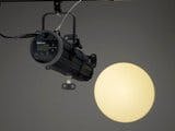
The second class of systems is sometimes called a spot light, and is distinguished by having a soft edge rather than the hard edge of profile projectors (Fig. 4). Soft edge spot lights are simple, very-narrow-beam systems. A common example of a soft-edge spot light is a tactical flashlight intended for illuminating objects at a great distance.
These nearly collimated light sources are sometimes said to be imaged at infinity. This characterization means that on the image plane, the source is imaged and a flashlight using a square LED will have a square shaped spot which can be aesthetically undesirable. As with the projectors, the beam geometry can be remedied by using a diffusing element or scattering surface on one of the optics. However, scattering spreads the beam and introduces system losses and reduced center beam candle power.
Life science applications
Benefits of round sources extend to non-imaging systems such as fiber-based systems, notably the ubiquitous 5-mm diameter fibers used in life sciences and medical endoscopy. Here maximum efficiency is achieved by optically coupling a round source to the round input face of the fiber bundle. Non-imaging optics such as compound parabolic concentrators (CPCs) or optical tapers are typically used to transfer the light from the LED to the fiber.
For reasons of manufacturability and cost, these optics are usually symmetric –meaning they consist of square input and output faces, or they consist of round input and output faces. To avoid optical loss due to a square mating with a circle, the highest efficiency solution is a round LED, round coupling optic and round fiber bundle. The traditional approach of using a square LED and overfilling the input aperture of the optic results in lost photons, while under-filling the optic results in a missed opportunity to inject more light into the fiber.
With system and optical efficiency gains to be had from round sources, you may ask why such products only recently came to market. Luminus' scientists knew that they could develop a round LED but needed to address cost as well as design. Fabricating a truly round die would require significant investment in capital equipment and process development. Simply singulating round die would be a financially flawed option.
Circular active area
The Luminus approach is to electrically isolate the die area outside of the circular shape on a square dire, and only power the round area. The immediate reaction to the idea of only injecting current in a round shape within a square die is always that it is an inefficient use of epitaxial real estate and therefore not cost effective.
If one stops thinking like a chip-head, however, and starts thinking like a designer of optical fixtures, you would note that your optical system is going to waste the lumens that would have been generated in the corners of the square, meaning you would be paying for real estate with no flux payback. In doing so, you would be consuming power and generating additional heat to burden the thermal design and/or reduce the LED efficacy. So in terms of system lumens, the round emitter is in fact more efficient in applications such as those described above.
The next challenge was to design a round product with the requisite performance and to develop the manufacturing capability. The largest die previously offered by Luminus was 12 mm2 in area. The flux goals of this program could not be achieved by pumping a circle within a 3.5×3.5-mm square die (emitting area of 9.4 mm2). It was determined that 14 mm2 of emitting area would be required which corresponds to a total square die area of 18 mm2. This represents a 50% increase over the previous Luminus platform, which is already many times larger than the industry standard.
Suitable optical emission uniformity over the circular area along with efficient current injection was required. This involved new optimizations for both n-ohmic and p-ohmic designs and bond pads. Iterative design led to selection of optimum tradeoffs between current handling capability, efficacy and uniformity. A large number of contact geometries were explored before the final geometry was selected for detailed design. Many of the design rules transferred from the existing Luminus Big Chip platform, but additional work was required to optimize for the circular symmetry.
Finally, such a product development must address design for manufacturability issues. Most wafer processes in use were scaled to the 18-mm2 die without issue. However Luminus equipment and processes for separating the LED from the sapphire substrate on which it is grown had reached their limits just beyond 12 mm2. Substantial capital investment and process development was required to enable these largest-ever LED die and now Luminus is, in principle, able to fabricate single die of any size or shape.
Circular benefits
For many general lighting applications, a square chip LED is adequate. However, in applications where maximum center beam candle power is vital such as spot lighting, entertainment lighting, medical device lighting, along with several other étendue limited optical architectures, round LEDs are best suited as the LED source.
Ultra-high lumen systems that are étendue limited would benefit most from these round emission LEDs. Additional potential applications on the horizon include high intensity transportation lighting, such as landing lights on aircraft, and narrow beam high intensity discharge (HID) replacement PAR lamps.
In the LED world, maybe we are beginning to see a shift in thinking outside the proverbial box. For example, consider a move toward creating an LED that is perfectly matched to an existing optical architecture rather than forcing the radical adaptation of a fixture's infrastructure just to be able to accommodate a standard LED light source.
Sidebar: Circular LED beams
There are an increasingly broad set of choices for product designs that need a circular beam pattern, despite the fact that most packaged LEDs use a square die. Indeed most smaller LEDs can be combined with a total-internal reflector (TIR) lens to form a circular pattern. For higher lumen output applications, the growing selection of multi-emitter LEDs provides more options.
As the main article mentions, most every major LED manufacturer offers chip-on-board (COB) arrays at this point. Bridgelux announced the Vero family recently with flux output as high as 20,000 lm. Cree recently added larger arrays in its CXA family that range to 5000 lm in light output.
While the COB approach typically involves mounting blue emitters in an array and covering the entire array with a phosphor slurry, Philips Lumileds took a different approach with its latest Luxeon S family. The LEDs use multiple phosphor-converted, high-power white LEDs discretely mounted on a small circuit board in a pattern that delivers a round beam (more on page 9).
