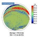
While the LED industry continues to march forward from a performance perspective using gallium-nitride-on-sapphire or gallium-nitride-on-silcon-carbide (GaN-on-SiC) technology, upstarts continue to believe silicon wafers hold the ultimate key to a reduction in LED costs and broader deployment of solid-state lighting (SSL). Azzurro Semiconductors is pursuing GaN-on-silicon (GaN-on-Si) template wafers and announced that it has achieved 3-nm wavelength uniformity in a production scenario and 1-nm uniformity in the R&D laboratory. Air Water, meanwhile, hopes to grow a SiC layer on Si wafers to reduce defects and yield LEDs with more light output.
The attraction of Si substrates remains low wafer costs, and the use of automated and depreciated IC fab lines for the back end of LED manufacturing processes. That said, at The LED Show, speakers said that LED component costs are a diminishing component in the SSL system bill of materials.
GaN-on-Si templates
We've previously covered Dresden, Germany-based Azzurro's strategy of building GaN-on-Si template wafers upon which LED manufacturers can grow their epitaxial GaN structures using their own intellectual property. Presumably Azzurro will handle the difficulties of manufacturing LEDs on silicon, including dealing with bowed wafers and variable wafer thickness.
At the recent International Conference on Nitride Semiconductors 2013 (ICNS-10) conference in Washington, DC, Azzurro announced its latest milestones. "We are very proud of our team’s record 1.0-nm achievement," said Azzurro co-founder Alexander Loesing. "With these results we show that our GaN-on-Si technology can bring the LED industry closer to the aim of making 1-bin LED wafers."
The lab development of 1-nm uniformity would yield 1-bin LEDs in terms of color, but Azzurro didn’t say when that achievement might be commercialized. Even the 3-nm-uniformity achievement in a production environment will lack some credibility until such LEDs are commercially available. Azzurro said that the achievement used 150-mm (6-in) wafers and also delivered forward voltage uniformity within 1.3%.
GaN-on-SiC-on-Si architectures
Air Water Inc, an industrial gas manufacturer based in Azumino, Japan, meanwhile, is working on a novel approach to using Si wafers by adding a SiC layer according to an announcement made by Aixtron, a maker of LED manufacturing equipment including metal organic chemical vapor deposition (MOCVD) reactors used to grow epitaxial layers in compound semiconductors. Aixtron said it installed an AIX G5 HT Planetary Reactor in an 8 wafer by 6-in configuration at Air Water's facility.
Cree has proved that SiC is an excellent substrate for GaN LEDs with the company consistently being at or near the lead in LED efficacy. SiC offers a better crystalline match between the wafer and the first GaN layer and therefore fewer defects and more light output. But the cost of SiC wafers is significantly higher than the cost of sapphire wafers, although Cree is clearly price-competitive using the technology.
The Air Water GaN-on-SiC-on-Si architecture presumably protects the Si wafer during the nucleation process. Meanwhile, the SiC layer would provide a better crystalline match to the GaN layers grown to form the LED structure.
Of course, the ultimate path in terms of homogeneity between substrate and epitaxial layers remains a GaN-on-GaN approach such as Soraa is pursuing. But GaN wafers are yet more expensive than SiC wafers.


