Despite double-digit growth rates and changes of focus in the LED industry, CAROLINE HAYES explains that the metal organic chemical-vapor deposition tool market has enjoyed moderate growth while the tools become more efficient and work with a variety of substrates.
While the power LED component market has increased its scope, moving from use in mobile phone, computer, and TV displays to general lighting, the increase in demand that this expansion has caused has not greatly impacted the companies that make metal organic chemical-vapor deposition (MOCVD) reactors required for epitaxial growth in LED manufacturing. Sales growth has been moderate, although the MOCVD makers have sought to minimize the time required for wafer-level epitaxy and also improve device uniformity. Moreover, the tool makers are dealing with the need for reactors to support varying wafer sizes and even substrates beyond the legacy sapphire that has been prevalent in the LED space.
Jamie Fox, principal analyst at IHS, explained why demand has not fueled a rush of orders. "If there is only a small increase in LED demand, manufacturers can keep up, using their existing machinery. Although LED demand has increased a lot, most companies have not added machinery but are trying to improve production efficiency." The cost of new equipment and the low margins for LEDs have kept LED manufacturers in a cautious mood. Fox said even companies with MOCVD machines at near-100% capacity often decide not to invest around $2 million in a machine and risk over-capacity if the market should suffer a downturn.
One company that has taken a bold step and invested in one of the largest MOCVD machine orders recently is Sanan Optoelectronics. The Chinese powerhouse for gallium-nitride (GaN)-based LEDs ordered 50 Aixtron MOCVD showerhead tools, for delivery from 4Q14. Companies like Aixtron in Germany and Veeco in the United States, which command around 90% of the MOCVD market, typically achieve two sales per quarter, according to Fox. The large Aixtron order will increase capacity for the leading wafer and die producer in China, and the substantial investment is a sign of confidence that orders will follow. Other commentators view it as part of China's bid to establish itself as "LED Valley," securing supply to companies in China that are manufacturing end products for companies in the West.
Four years ago, LEDsMagazine reported a potential glut in the LED market as companies in China placed multimillion-dollar orders for multiple MOCVD reactors. That report was based on research by analysts at Strategies Unlimited. Since then, activity has waned. Sanan's order came too late to be included in Aixtron's latest financial results; it will be included in the next quarterly report.
Aixtron reported an increased loss in 3Q14 (to September 2014) of €17.9 million ($20.3M) from €10.6M ($12M) in 2Q14. The company reported increased customer interest for its non-LED technologies, i.e., power management devices. Aixtron has observed that its LED customers face "competitive industry dynamics."
Substrate choices
The GaN LED market is a substantial one, estimated to be worth $14.4 billion in 2013 and forecast to be worth $25.98B in 2018, according to Strategies Unlimited. GaN MOCVD shipments are projected by IHS' Fox to be 254 reactors in 2014, most of these in Asia.
Most white power LEDs are GaN-based, with the majority of these produced on sapphire substrates. There is also GaN-on-SiC (silicon carbide) and GaN-on-Si (silicon). A fourth option is GaN-on-GaN, as used by Soraa, the LED company that was co-founded by Shuji Nakamura. Nakamura won the Nobel Prize in Physics with professors Isamu Akasaki and Hiroshi Amano for developing the first blue LEDs, which, when combined with phosphor, yield white light.
Wafer or substrate sizes vary significantly. GaN-on-Si upstarts are focused on 8-in. or larger wafers, hoping to use mainstream semiconductor fabs for the back-end of manufacturing after epitaxial growth in MOCVD reactors. Sapphire LED makers are moving from 2-in. to 4-in. wafers and will ultimately go larger. The epitaxial production processes for all technologies are similar and use the same deposition methods.
Tool maker impact
There has been some movement in the amount of companies using the various substrates, said Jim Jensen, senior vice president of MOCVD technology and business at Veeco. The company lists Osram, Epistar, Samsung, LG, and Seoul Semiconductor among its customer base. The majority of customers in the LED space (more than 90%) use GaN-on-sapphire, noted Jensen, but there has been a slight shift in the last five to ten years. The cost of GaN still means that GaN-on-GaN is used by only one or two customers, "in meaningful amounts," he said, but for GaN-on-Si, it has changed from a lot of R&D activity and zero production years ago to less R&D and more production; but GaN-on-Si is still confined to two or three customers.
Silicon is a cost-effective option for many manufacturers because, as mentioned previously, it allows the use of existing IC manufacturing equipment and techniques. The lattice mismatch between GaN and the silicon, however, requires a buffer layer to compensate for the misalignment. This may add complexity and some cost, but it is perceived as being outweighed by the economies of scale afforded by both the low initial cost of silicon wafers and reuse of equipment.
At the moment, Cree stands alone, promoting its GaN-on-SiC technology, while Soraa promotes the GaN-on-GaN LED architecture as having a "near-perfect" crystal structure. The homogenous wafer and growth layers result in the ability of an LED chip to support a higher power density and produce more light from a smaller area.
"GaN is interesting," said Jensen. "It is more efficient, produces higher yields and ultimately brighter devices, but it is prohibitively expensive." Without a dramatic change in pricing, to overcome the x100 price tag compared with sapphire, or the possibility of reuse, he does not see its use increasing.
GaN-on-Si prospects
Two years ago, Aixtron addressed GaN-on-Si technology with the introduction of the AIX G5+, 5×200-mm hardware and process capabilities for the AIX G5 planetary reactor. These capabilities are now available as part of the company's AIX G5 family.
For the German company, GaN-on-Si is a focus area. Rainer Beccard, vice president of marketing for Aixtron, said at the G5+ introduction that GaN-on-Si is "a very promising candidate for future high performance and low cost high-brightness LED (HB-LED) manufacturing." He went on to say that the transition to 200-mm (8-in.) standard silicon wafers with the G5+ is the next logical step "as it offers unique economies of scale," referring to wafer size and material for cost-effective manufacturing processes. The larger wafers translate into lower cost of ownership enabled by more die per wafer.
Yield is not the overriding issue for the MOCVD market. Uniformity ranks high as it enables LEDs with matching flux and color profiles. In turn, uniformity increases productivity and therefore reduced manufacturing costs.
For the AIX G5+, initial customer feedback notes that the fully rotationally symmetrical uniformity pattern on all five 200-mm wafers, the use of standard-thickness silicon substrates, and the controlled wafer box behavior is "exactly what they require for a silicon-style manufacturing." Being able to obtain uniformity pattern on 200-mm GaN-on-Si wafers is seen as a mark of success in technological development.
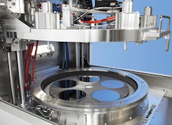
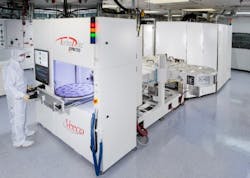
Veeco tells the same story: Uniformity and capacity are paramount. Its TurboDisc EPIK700 GaN MOCVD system more than doubles capacity of the earlier-generation machine. It is available in one- and two-reactor formats and can accommodate 31 4-in. wafers on each reactor, for a total of 61 wafers on the two-reactor model. It accommodates six 8-in. wafers per chamber, or 12 wafers on the two-reactor model, or 12 6-in. wafers/24 for the two-reactor version. The company estimates that it can achieve a cost-per-wafer savings of up to 20% compared to the previous generations by virtue of improved wafer uniformity, reduced operating expenses, and increased productivity.
General lighting market
The transition to LED use in general lighting applications has also impacted the MOCVD tool makers. In general lighting LEDs, advances have required efficient capital investment, cost of ownership, and performance in terms of throughput and uniformity, said Jensen. He summed it up as "Efficiency of capital is [the calculation of] wafer, per day, per dollar.
"Customers always push suppliers on uniformity," added Jensen, "heightening the specs." This is not expressed in a single formula, he noted. Some customers measure uniformity in percentages or in terms of sigma measurement or wavelength uniformity - depending on the process the customer uses. The EPIK700 uses both IsoFlange center injection flow technology to control the flow of gas onto the substrate and the disk, and the TruHeat wafer coil to control temperature and provide a homogeneous laminar flow and uniform temperature across the entire wafer carrier.
Another relatively recent change is the vogue in wafer sizes. "Five years ago," explained Jensen, "the majority was 2-in. wafers, with 4-in. wafers pushing through and some 6-in. [wafers]. Now there is a few more 6-in. wafers, the majority is 4-in. wafers, perhaps 40%, with less than 5% being 8-in. GaN-Si wafers" and the balance being 2-in. wafers.
Wafer sizes may change, bringing some adjustments to MOCVD equipment, but equipment companies are also introducing change at the pace expected of a reasonably mature market. It is subject to the end goals of customers who strive to maximize capital efficiency while competing on price in a consumer-driven end market.
CAROLINE HAYES is a contributing editor with LEDs Magazine.


